S4.2 Pins should be grouped by function
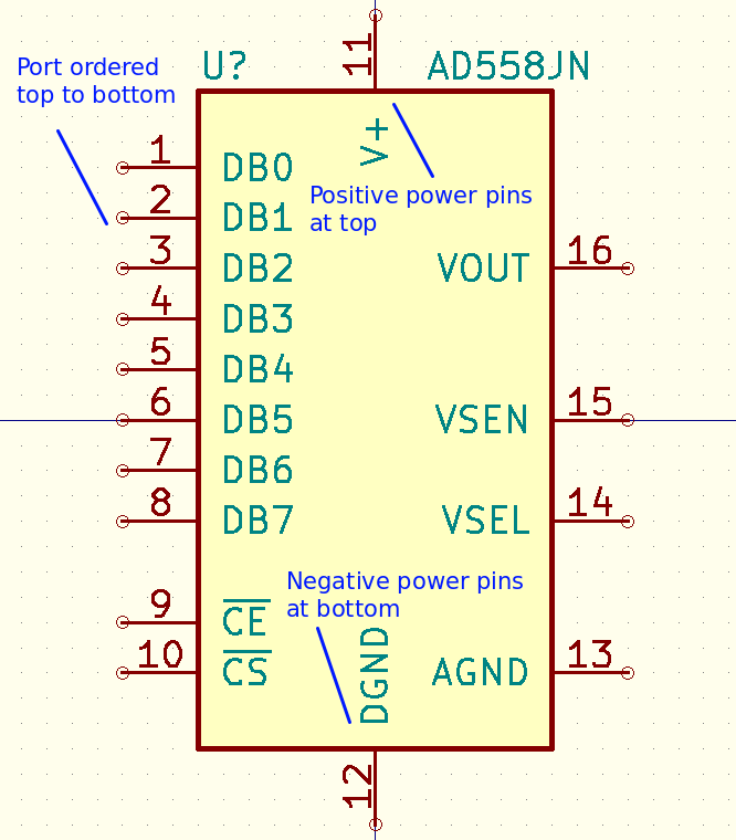
Where possible, pins should be grouped by similar function, rather than by their physical location on the associated footprint. This provides cleaner schematic routing and symbols are easier to understand in the schematic.
-
Pins with similar functions should be grouped together:
-
SPI_MISO,SPI_MOSI,SPI_CS,SPI_CLK -
UART_TX,UART_RX
-
-
Ports should be ordered from top to bottom
-
Positive power pins should be placed at the top of a symbol
-
Vcc,Vdd,Vin,V+, etc.
-
-
Negative power and ground pins should be placed at the bottom of a symbol
-
GND,Vss,V-, etc. -
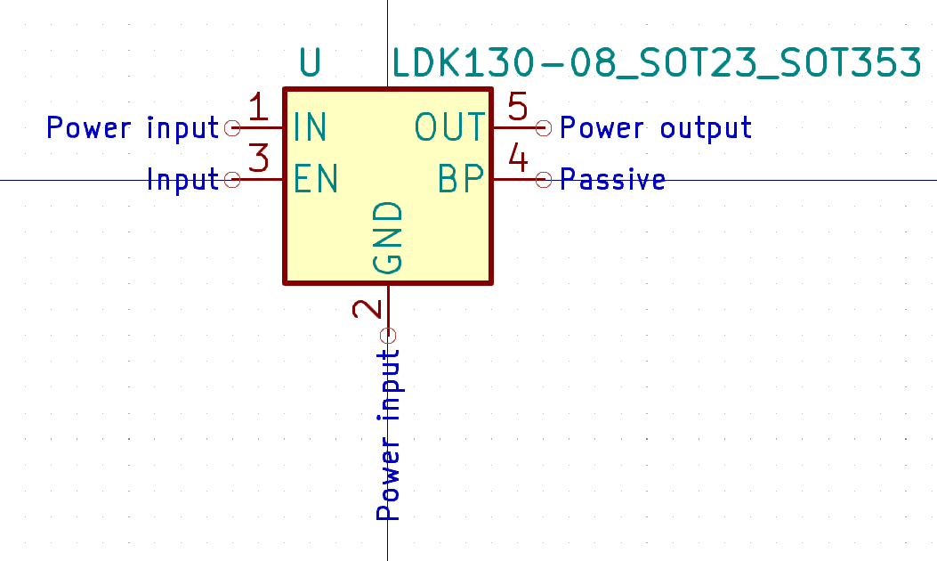
Exception Devices intended for power conversion that have both a power in- and output should have the power input pins on the left and the power output pins on the right.
-
-
Input/Control/Logic pins should be placed on the left of a symbol
-
Enable,Sleep -
Iset
-
-
Output/Controlled/Driver pins should be placed on the right of a symbol
-
Alarm -
ChargeFinished -
Q,!Q
-
-
Bus connections like SPI/I²C/.. should be arranged according to library standards (Examples can be found in the wiki, https://gitlab.com/groups/kicad/libraries/-/wikis/Symbole-Bus-Pin-Order)

