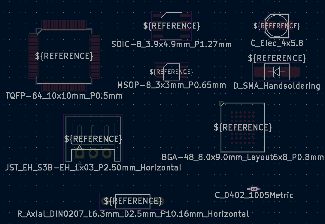
F5.2 Fabrication layer requirements
The fabrication layers are used to display the simplified mechanical outline of components on the PCB.
KiCad refers to the fabrication layers as:
-
F.Fab- Front fabrication layer -
B.Fab- Back fabrication layer
The following elements must be provided on the fabrication layer(s)
-
Simplified component outline must be provided on
F.Fablayer-
Outline uses line width between {
0.10mmand0.15mm} (recommended0.10mm) -
Outline should be simplified and not display complex features
-
For outlines based on the component body shape, the nominal size is used
-
-
Footprint polarisation / location of pin-1 is drawn
-
For IC packages, bevel is drawn at corner next to pin-1
-
Bevel should be
1mmor25% of package size(whichever is smaller) -
For connectors, a small arrow indicator drawn next to pin-1 should be used
-
-
Component value (footprint name) must be displayed on the
F.Fablayer-
Recommended text size =
1.0mm -
Allowable text size = {
0.5mmto1.0mm} -
Text thickness should be approximately
15%of text size ( with allowances for variation for aesthetic reasons) -
Placed below (positive y direction) the part outline.
-
-
A second copy of the reference designator (RefDes) must be provided on the
F.Fablayer. To add a second RefDes item, add a text object with the value${REFERENCE}-
RefDes must be centered on component body (inside component outline)
-
Orientation of RefDes should match major component axis
-
Size of text should be scaled to match component size
-
It is recommended to scale it such that 4 characters fit without overlapping other features of the same layer.
-
If it is not possible to fit at least 3 characters with the text size restrictions, then the reference should be moved outside (but scaled to smallest allowable text size)
-
-
Recommended text size =
1.00mm -
Allowable text size = {
0.5mmto1.0mm} -
Text thickness should be approximately
15%of text size (with allowances for variation for aesthetic reasons)
-
