F5.3 Courtyard layer requirements
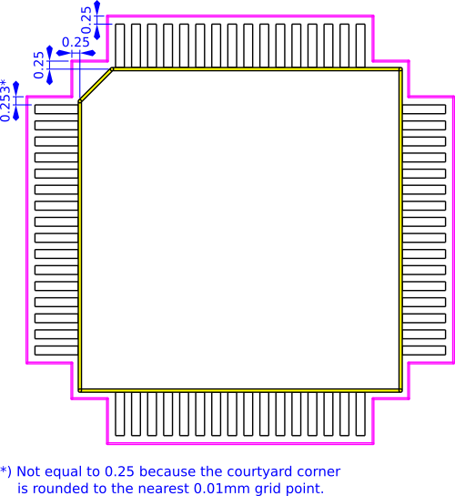
The component courtyard is defined as the smallest rectangular area that provides a minimum electrical and mechanical clearance around the combined component body and land pattern boundaries. It is allowed to create a contoured courtyard area using a polygon instead of a simple rectangle. (IPC-7351C)
The courtyard should include any extra required clearance for mating connectors (for example).
KiCad refers to the courtyard layers as:
-
F.CrtYd- Front courtyard layer -
B.CrtYd- Back courtyard layer
A fully enclosed Component courtyard must be drawn on the F.CrtYd layer, with the following parameters:
-
Courtyard uses
0.05mmline width -
All courtyard line elements are placed on a
0.01mmgrid -
If the component requires a courtyard on the back of the PCB, a corresponding courtyard must be provided on the
B.CrtYdlayer. -
Where the courtyard depends on the dimensions of the physical part body, clearance is calculated from the nominal part dimensions.
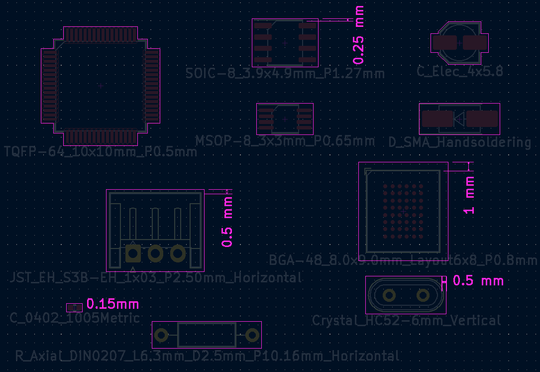
Courtyard clearance should adhere to the following requirements:
-
Unless otherwise specified, clearance is
0.25mm. This shrinks to0.15mmfor parts smaller than 1.5mm in any dimension. -
(retracted)
-
Connectors should have a clearance of
0.5mm, in addition to the clearance required for mating of connector -
Canned capacitors should have a clearance of
0.5mm -
Crystals should have a clearance of
0.5mm -
BGA devices, including WLCSP and similar, should have a clearance of
1.0mm.
Example for courtyard clearance when applied to the contoured courtyard outline of a QFP-64 package. (Shown are courtyard, fab-outline and copper pads.)

