F5.1 Silkscreen layer requirements
The silkscreen is printed to the external surface of a PCB to aid in component identification and orientation. Typically this layer contains the component RefDes to locate components on the board after assembly.
KiCad refers to the silkscreen layers as:
-
F.SilkS- Front silkscreen layer -
B.SilkS- Back silkscreen layer
The following elements must be provided on the silkscreen.
-
Reference Designator must be drawn on
F.SilkSlayer-
Text size =
1.00mm -
Text thickness =
0.15mm
-
-
Silkscreen line width is between {
0.10mmand0.15mm}:-
Silkscreen line width should nominally be
0.12mm -
0.1mmis allowed for high density designs -
0.15mmis allowed for low density designs
-
-
Silkscreen must not be placed over pads or areas of exposed copper
-
Clearance between silkscreen and exposed copper elements is recommended to be 0.2mm.
-
Clearance must be at least the silkscreen line width or pad mask expansion, whichever is greater.
-
-
For SMD footprints, silkscreen must be fully visible after boards assembly (no silkscreen allowed under component)
-
For THT components, additional silkscreen may be placed under component to aid in assembly process
-
Polarity marking / Pin-1 designator must be drawn on the
F.SilkSlayer -
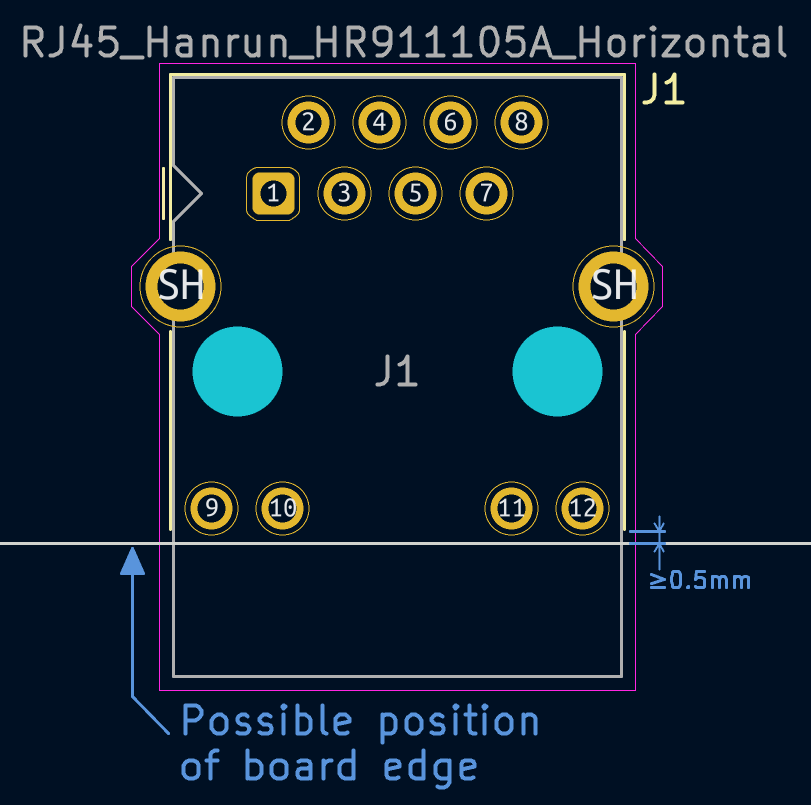
When components are expected to protrude past the board edge (e.g. connectors), silkscreen should not be placed such that a reasonably-placed component has silkscreen outside the board
-
Clearance between silkscreen and board edges should be at least 0.5mm
-
Polarity marking / Pin-1 designator
-
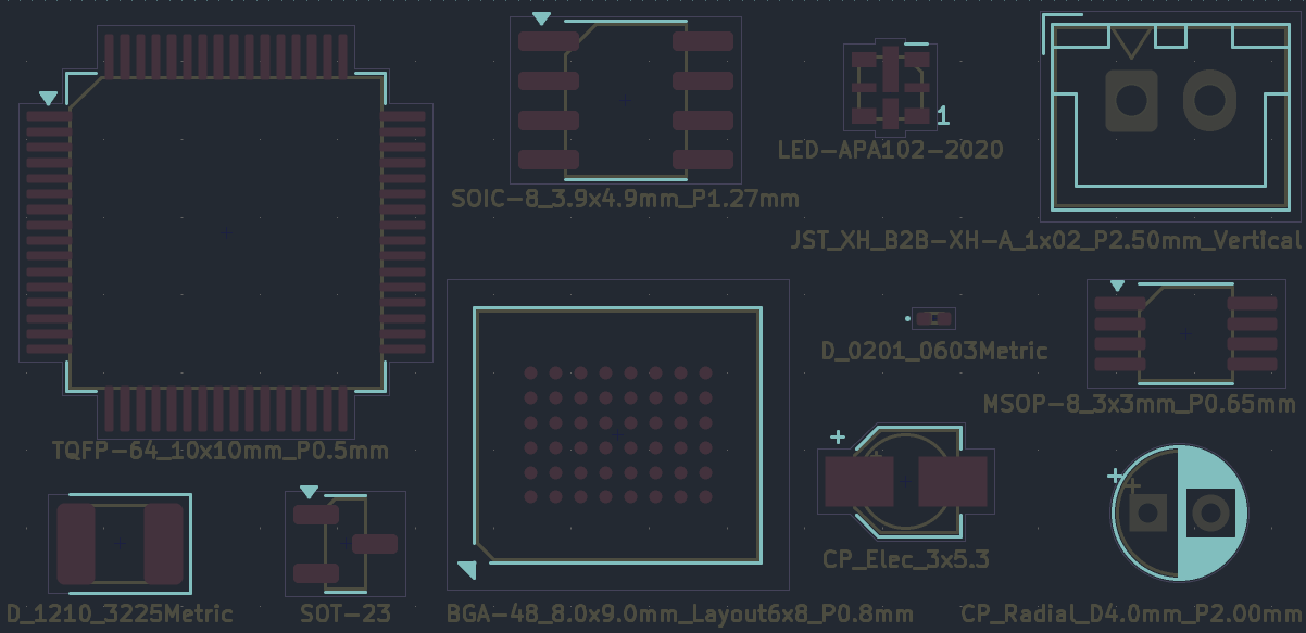
The prefered style for SMD packages is a filled chevron
▶-
It should positioned inside the courtyard to prevent silkscreen overlap
-
It can be rotated by 45° for a better fit
-
-
Examples other established and acceptable styles
-
for SMD devices
-
⊔shape for SMD diodes -
For small packages (0201 diodes, …) a 0.25mm dot should be used.
-
-
for THT and SMD packages
-
corner bracketorextra linefor connectors -
+sign for SMD capacitors
-
-
Follow established styles that already exist in the target library
-
-
If the device has a marking that is not on Pin-1 (popular on digital LEDs), the marking needs special attention
-
The digit
1is put on the silkscreen marker next to the pin numbered 1 -
The silkscreen polarity marking is placed according to the physical marking on the device
-
-
The marking must be visible after board assembly for inspection and debug purposes
-
It also should be visible after connector mating
-
Examples
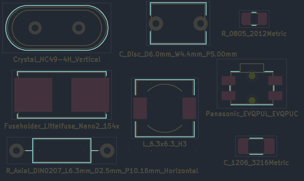
Examples of silk for non-polarized components
Examples of silkscreen for polarized components
Example of a connector with silkscreen that is "pulled back" from possible board edges:


