*.kicad_mod textThe KiCad Library Convention (KLC) is a set of requirements for contributing to the official KiCad libraries. Users wishing to submit or update library files should be familiar with these guidelines.
The KLC are a set of guidelines, rather than rules. Electronic component libraries are diverse and complex, and exceptions can be made at the discretion of the library team.
Where the KLC deviates from a particular datasheet or manufacturer recommendation, the datasheet should take preference unless there is a good reason not to do so (which should be clarified by a librarian).
Where the KLC is unclear, users should attempt to match the convention of existing library components, or seek further clarification.
Refer to the contribution guidelines for introductory information on contributing to the KiCad libraries.
KLC Helper Scripts
The KiCad library team has developed a set of Python scripts which can be used to help test if library components conform to the KLC requirements.
When a merge request is made to the libraries, the contributed files are automatically checked using these scripts. It can be helpful to run these scripts on your local machine before submitting a PR, as it will help speed up the process of merging your contribution(s) into the library.
To run the footprint checker script, for instance, cd into the "kicad-library-utils/klc-check" directory, then run the Python script ./check_footprint.py path_to_fp1.kicad_mod path_to_fp2.kicad_mod -vv. This will carefully check your footprint according to the KLC requirements laid out below, notifying you of any discrepancies, errors, or violations. See more usage examples in the readme at the link above.
Note: While many of the KLC guidelines are checked by these scripts, there are some which are not covered. Additionally, any PR requires manual checking by a member of the library team.
GitLab Wiki
The KLC provides a comprehensive foundation for anyone contributing to the official KiCad libraries. However, the KiCad Libraries GitLab Wiki serves as an invaluable addition to the KLC website.
The GitLab Wiki offers resources that go beyond the formal guidelines, including:
-
Practical guidance: Detailed explanations on applying KLC guidelines in typical projects, along with specific examples and best practices
-
Community contributions: Frequently updated tips and information contributed by the community, helping users avoid common mistakes and troubleshoot issues
-
Exceptions and clarifications: Guidance on specific cases where deviations from the guidelines are sensible or necessary
Anyone reviewing the KLC website should also explore the GitLab Wiki to gain deeper insights into guideline application and access useful tools and extended information for a smoother contribution process.
Refer to the KiCad Libraries GitLab Wiki for more details.
General Library Guidelines
The general library guidelines apply to all library elements (symbols / footprints / models / templates / 3D models). However, these guidelines may be overridden in some cases by specific exceptions described in further sections.
G1 - General Guidelines
G1.1 Only standard characters are used for naming libraries and components
Filenames, symbol names, footprint names, model names, 3D model names, and template names must contain only valid characters, as determined below:
-
Alphanumeric characters (
A-Z,a-z,0-9) -
Underscore
_ -
Hyphen / dash
- -
Period / dot
. -
Comma
, -
Plus symbol
+
This character set ensures that symbols will be compatible with all filesystems, and will not cause any issues due to character rendering.
Further, filenames and symbol names must not use the space character. This can cause issues with string escaping and is best avoided.
G1.2 Withdrawn
This rule was withdrawn.
G1.3 Libraries are organized by functionality
Rather than grouping components (e.g. symbols, footprints) by their manufacturer, KiCad libraries are organized by component functionality. This grouping strategy has a number of key benefits:
-
Similar components are grouped together, allowing alternative parts to be easily substituted
-
If possible, symbols should be derived from existing symbols to reduce library size
-
Generic parts which are produced by multiple manufacturers are supported
Library organization should follow the general form as described below, with each element separated by the underscore (_) character:
-
Library function
-
Library sub-function
-
Tertiary qualifier
-
Manufacturer name
-
Component series name
-
Extra library descriptors
Note: Some of the elements listed above may be omitted if not required.
For specific examples, refer to the guidelines for organizing symbol libraries and footprint libraries.
G1.4 English language should be used throughout libraries
KiCad software is used by people who speak many different languages. The KiCad software provides translations for these languages, but the library files do not provide translations.
Library files should be written using English, excepting where specific component names are non-English (for non-English manufacturers).
Where potential differences in spelling and grammar exist, American English should be given preference.
-
Colorinstead ofColour
G1.5 Plural naming is to be avoided
In general, plural naming (e.g. for libraries) should be avoided, as pluralisation of some words is inconsistent. Non pluralized names should be used in preference:
-
Sensor_Temperatureinstead ofSensors_Temperature -
Memory_Flashinstead ofMemories_Flash -
TerminalBlockinstead ofTerminalBlocks
G1.6 Capitalization conventions
-
Acronyms should be capitalized
-
MCU(microcontroller) -
FPGA(field programmable gate array)
-
-
Manufacturer names should be capitalized according to the manufacturer
-
Microchip -
ROHM -
Texas -
NEC
-
-
Unless separated by delimiters such as
_,-,., words should be separated using CamelCase convention, with the first letter of each word capitalised-
TestPoint -
BatteryHolder
-
G1.7 Library files use Unix style line endings
Library files must always be commited to GitLab using Unix-style line endings. This means that lines are terminated using the LF (line feed) character, rather than the DOS style CR+LF line endings.
KiCad library files must be compatible across multiple operating systems, and users should be able to contribute without generating unnecessary noise in the files by constantly changing line endings.
When using the KiCad libraries on a Windows PC, the line endings in the library files may be automatically converted to CR+LF. This is fine, as long as any contributions made to the libraries observe the LF line ending requirements.
This issue is addressed by insisting that all KiCad libraries include a .gitattributes file. This file ensures that the line endings are automatically converted by Git.
An example of a simple .gitattributes file which ensures footprint files have correct line endings is as follows:
Note: The KiCad library repositories should already have the correct .gitattributes file in place to achieve this
G1.8 Contributions to the official library must be made using the current stable version
Contributions of library assets must be created in the latest stable version of KiCad.
This is to avoid problems caused by changes in how assets are stored in different versions of KiCad. (Changes in how line ordering is determined, how strings are escaped, etc.) Another reason is to avoid including features not supported by the latest stable release.
G1.9 Dimensional units
-
When specifying a dimension (e.g. in a footprint name) the units must always be provided:
-
3mm- millimeters -
1in- inches
-
-
When specifying areas or volumes, the coordinate order is
X-Y[-Z], which is equivalent towidth-height[-thickness]. -
When specifying multidimensional units (e.g.
widthxheightxthickness) then the units only need to be appended once-
3x4x7mm- 3mm x 4mm x 7mm
-
-
Metric units are preferred, where appropriate
-
Linear dimensions should be specified in millimeters
-
Angular dimensions should be specified in degrees
-
Temperature should be specified in degrees Celsius
G1.10 Embedding files
Symbols and Footprints must not contain embedded files. Thus the embedded fonts checkbox also should never be set.
The feature is intended to embed datasheets, 3D-Models or fonts. All of those most likely are not compatible with the library-license. Also, this would vastly increase the file size of the repositories.
Possible exceptions from this rule: . Spice models in symbols
G2 - Generic and Fully Specified Symbols
G2.1 Definition of terms: Generic and fully specified symbols
KiCad has two workflows regarding what a symbol represents and when it is assigned a footprint. It can be done in the library in which case the symbol represents an exact part or using the "Assign Footprints" tool at the end of the design process.
Generic symbols
Generic symbols can be used with multiple footprints. They do not have a default footprint assigned. Generic symbols allow flexibility in the design workflow. For this workflow the symbol placed into the schematic is typically selected to fit the intended function instead of fitting a particular part. The footprint assignment happens later when the exact part number is selected. Using generic symbols allows a small number of library symbol elements to represent a very large number of possible component combinations.
An example of the use of generic symbols are the Resistor and Capacitor symbols available in the KiCad library. These symbols do not have an assigned default footprint, as there are many possible compatible footprints.
Fully specified symbols
Fully specified symbols define a matching footprint, and are named based on the MPN (manufacturer part number). Such symbols do not depend on the user to select the correct footprint later but can have alternative footprints defined using footprint filters such that the user can select an alternate footprint.
A fully specified symbol together with a footprint specialized to one component are called an atomic part. A library of only such parts is called an atomic library. Confusingly, some users refer to a fully specified symbol as an atomic symbol.
Where to use which type
The official library requires fully specified symbols except for a small number of libraries that contain only generic symbols. These generic libraries are:
-
Device -
All
Connectorlibraries -
The logic family libraries like
74xx,4xxx, …
G3 - Special Pin Numbering
G3.1 Relays
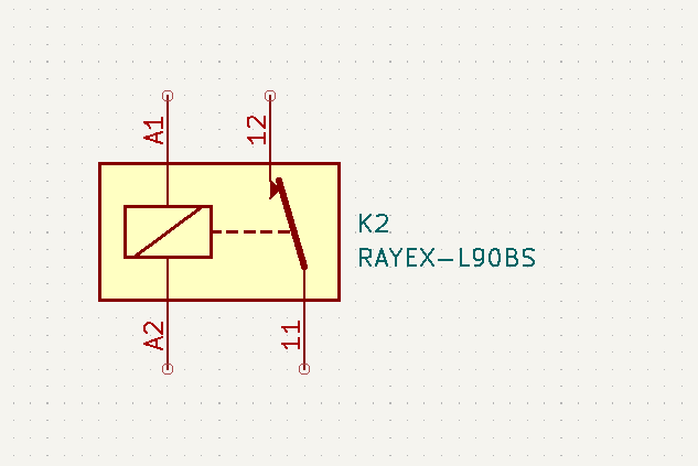
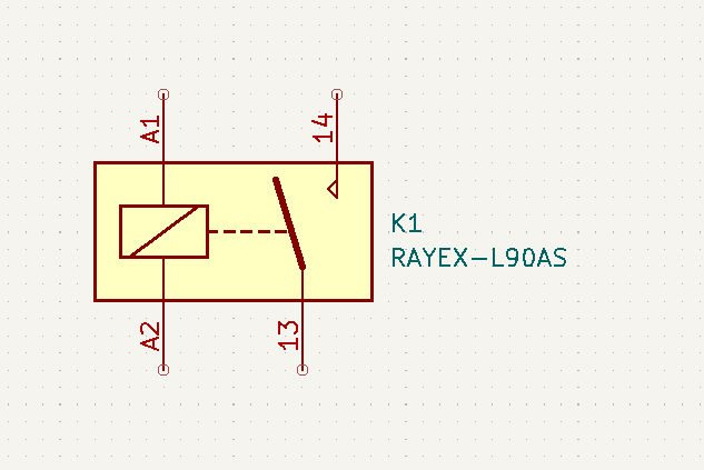
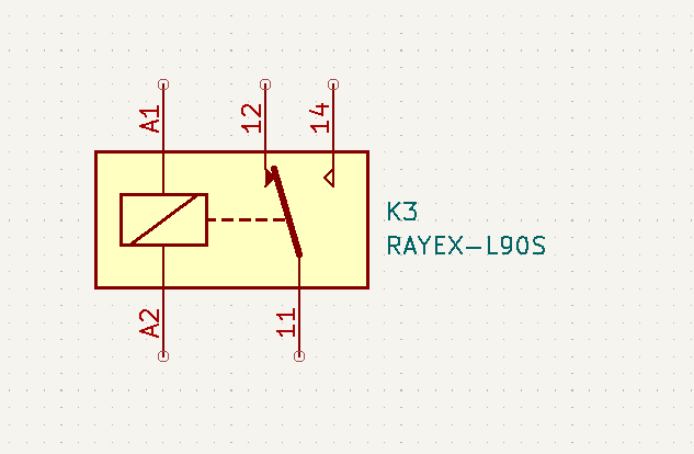
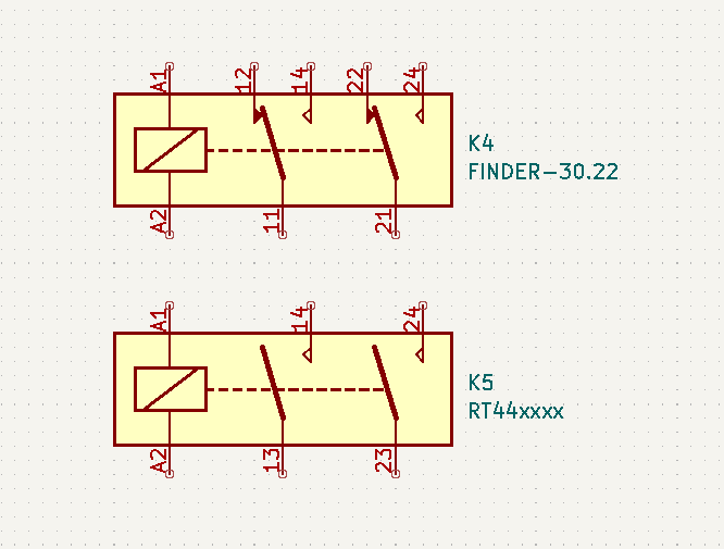
Pin numbers for relays follow EN 50005.
-
The coil contacts shall be named
A1andA2.-
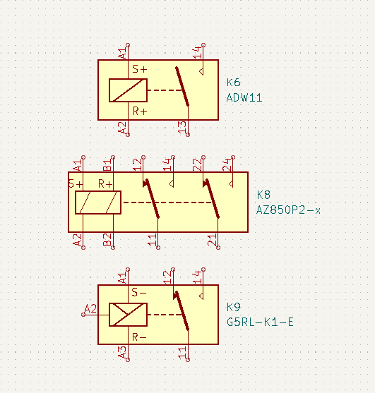
For more complex relay magnetics, each coil pin shall have a letter and a number. The letter shall describe which coil the pin belongs to; the digit shall describe the tap number in that coil.
-
Bistable relays shall have current flowing at the A1 pin in the A coil
Setthe relay and be labelledS+orS-. -
Bistable relays should be labeled
R+orR-in theResetcoil or direction as well. -
In Bistable relays, labeling the positive direction that the current flows from shall be preferred over labeling the negative direction that the current flows to. Where it is not possible to label the positive direction, such as center-tapped relays with current always flowing from the center tap, the negative direction should be labelled.
-
-
Contacts shall have two digits each. The first digit shall be the index number of the pole group; the second digit shall describe the function.
-
Normal-Close (NC) contacts shall be
x1andx2 -
Normal-Open (NO) contacts shall be
x3andx4 -
Changeover contacts shall be
x1for the common contact,x2for NC, andx4for NO
-
NC Contacts Example
NO Contacts Example
Changeover Contacts Example
Multiple Poles Example
Bistable Relay Example
G3.2 Audio Connectors
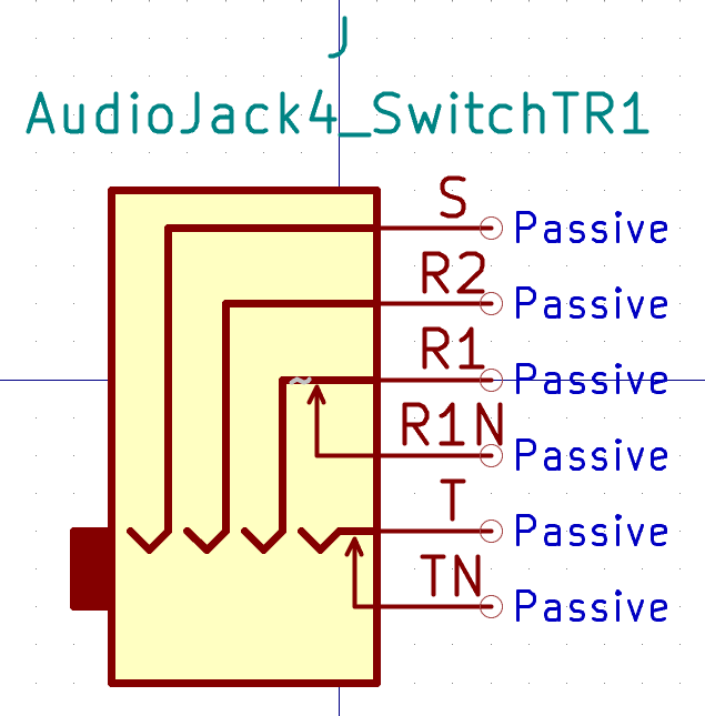
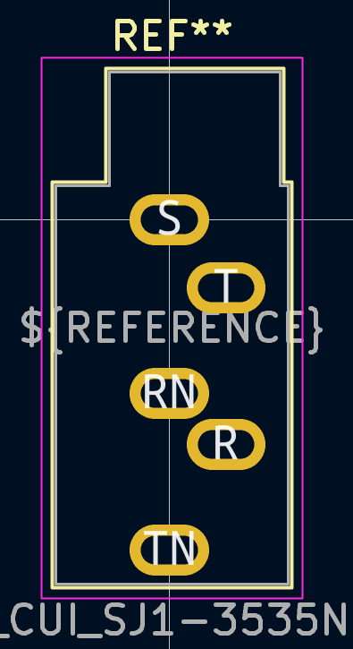
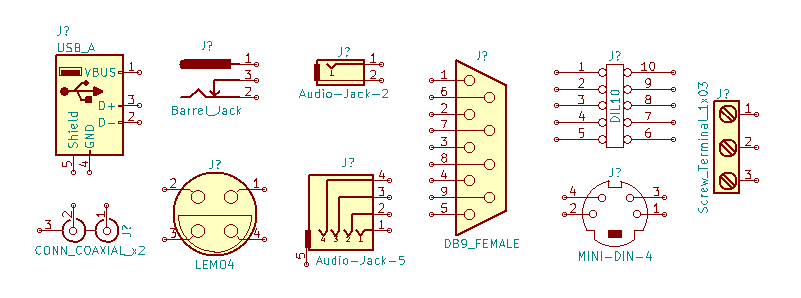
Audio jacks have specific pin names which are industry-standard and broadly understood. By giving the symbols and footprint the same generic pin names, a single generic symbol can be used for a variety of footprints without needing many manufacturer-specific symbols.
-
The basic pin names are "T" (tip), "R" (ring), and "S" (sleeve). "R" is used for stereo or balanced systems and is not always present.
-
Multiple ring connections may be used, and in that case they are named "R#" where "#" is a number starting at 1, with "R1" closest to "T". See AudioJack5 for a symbol with three ring terminals.
-
Some pins may be "normalled" (or switched) meaning signal flows through the connector when no jack is inserted, and the signal path is broken and re-directed from the jack when it is inserted. The normalled pins are given a suffix "N" after the name of the pin they switch. `AudioJack4_SwitchTR1' shows the "T" and "R" pins being switched.
Footprints covered by this rule should not have a polarity/pin1 marking. This overrides the F5.1 rule.
Note that XLR connectors have standard pin names of 1, 2, and 3. Combination jacks will when use both letters and numbers. An example of this symbol is XLR3_AudioJack3_Combo.
Examples
Symbol Guidelines
The following guidelines apply to schematic symbols and symbol library files.
S1 - Symbol Libraries
S1.1 Symbol libraries should be categorized by function
Symbol library names must be defined based on the priority list below, with each element separated by the underscore (_) character:
-
Function (e.g.
Sensor,Amplifier,MCU) -
Sub-function (e.g.
Temperature,CurrentSense) -
Tertiary qualifier (e.g.
CMOS) -
Manufacturer name (e.g.
Atmel,Infineon) -
Symbol series name (e.g.
PIC24,STM32) -
Extra library descriptors (e.g.
Deprecated)
Note: Some of the elements listed above may be omitted if not required.
Example symbol library names:
-
Power_Monitor- Power monitoring components -
Sensor_Temperature- Temperature sensors -
Driver_Motor- Motor drivers -
MCU_Microchip_PIC32- PIC32 microcontrollers from Microchip
S2 - Symbol Naming
S2.1 General symbol naming guidelines
-
Library naming should not be duplicated in symbol name
-
If symbol with same name exists for multiple manufacturers, the manufacturer name is written first
-
Fully specified symbols are named based on the manufacturer part number
-
If multiple manufacturers produce compatible parts but their part number suffixes for specifying the package differ, then the common base part number is used with clear name suffix for the footprint (e.g.
L78L05_TO92) -
Non-functional parts of the MPN must be replaced with a wildcard. (Refer to requirements for the use of wildcards in MPN)
-
-
Generic symbols use the device type
-
May be shortened for common components (e.g.
ConnforConnector) -
Reference designator may be substituted for common components (e.g.
D,C,LED)
-
-
Indicate quantity of elements for symbol arrays (e.g. resistor array with 8 elements -
Resistor_x8) -
Any modification of the original symbol, indicated by appending the reason
-
Different pin ordering -
Q_NPN_CBE,Q_NPN_BCE -
For multi-unit variants of typically single-unit symbols add the suffix
_Split
-
S2.2 Non-functional variations in part number should be replaced with wildcard
Manufacturer Part Numbers (MPN) often include variations that are non-functional in terms of schematic entry and PCB layout.
Examples of parameters considered non-functional:
-
Temperature rating of the component
-
Packaging information (e.g. reel, tray, tape)
-
RoHS / PbFree information
Examples of parameters considered functional are those that affect the schematic or layout of the part:
-
Electrical variations - these indicate important different characteristics (e.g. different supply voltages)
-
Package options - these indicate different footprints and/or pinouts
To capture every possible combination of part variation would require a large number of derived symbols and is to be avoided.
-
Where an MPN has options for such non-functional variations, these portions of the MPN should be replaced with the wildcard character (lowercase
x).-
If these non-functional parts of the MPN are at the end of the symbol name then the wildcard should be omitted.
-
-
Functional variations should be captured in the symbol name.
-
If there’s only one functional variation of the part, the wildcard does not need to be applied
-
Example:
TPS3430has only one variant:TPS3430WDRCR. So the name should beTPS3430WDRC, rather thanTPS3430xDRC.
-
S2.3 Where parts are available in multiple footprint options, a separate symbol must be drawn for each footprint
Many electronic components are provided in multiple packages. These may or may not be pin compatible.
Fully specified symbols require a separate symbol for every package. If they are pin compatible, the derive from existing symbol function must be used. Footprints in KiCad have a 1:1 relationship with their 3D model. This means multiple footprints are required where the 3D model has functional differences even if the footprints are identical (for example when 3D model height differs).
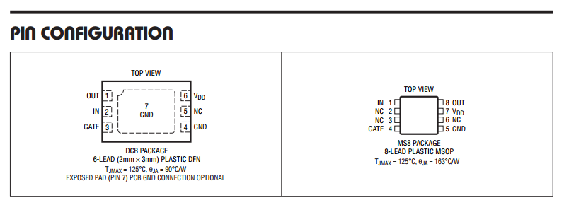
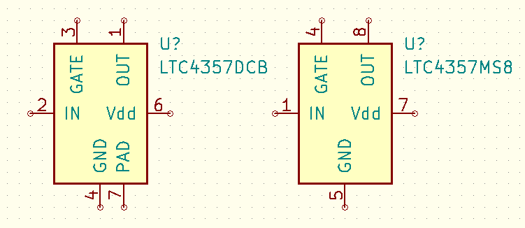
e.g. LTC4357
This part comes in two distinct packages each requiring a separate footprint. Hence a symbol for each variant must be drawn.
For naming of the symbols refer to General symbol naming guidelines
Where possible, the symbols should be drawn such that they can be swapped in the schematic with minimal disruption to wire connections.
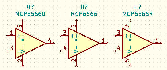
As a further example we shall consider the comparator MCP6566 which is available in three SOT-23-5 versions, each with a different pinout.
In this case, a separate symbol must again be drawn for each version, and named according to the convention called out in the datasheet.
S3 - General Symbol Requirements
S3.1 Origin is centered on the middle of the symbol
For symmetrical symbols, the symbol must be centered around the origin (0, 0) in the symbol editor.
Exception:
For non-symmetrical symbols, or symbols where this requirement would move pins off the 100mil grid, then the symbol should be placed as close to the origin as possible while observing the pin grid alignment requirements.
S3.2 Text fields should use a common text size of 50mils
-
All text fields (pin name, pin number, value, reference, footprint, datasheet) should use a text size of
50mil(1.27mm). -
Pin names and pin numbers can use a text size as small as 20mil if the symbol is small or has special geometry.
S3.3 Symbol outline and fill requirements
-
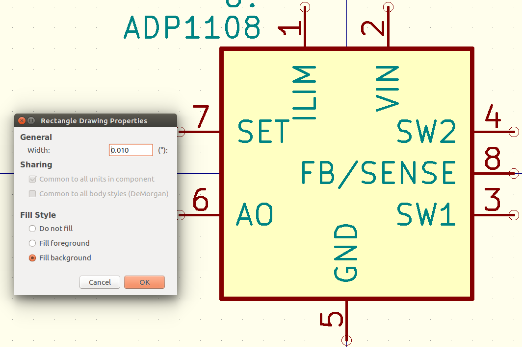
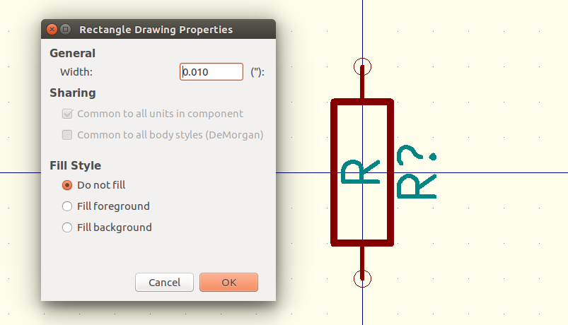
Symbol body must have a line width of
10mil(0.254mm) -
Black-box symbols (e.g. ICs with hidden functionality) should be filled with background color
-
Simple components (e.g. discrete components or those with a distinctive shape) should not be filled with background color
Fill background
Do not fill
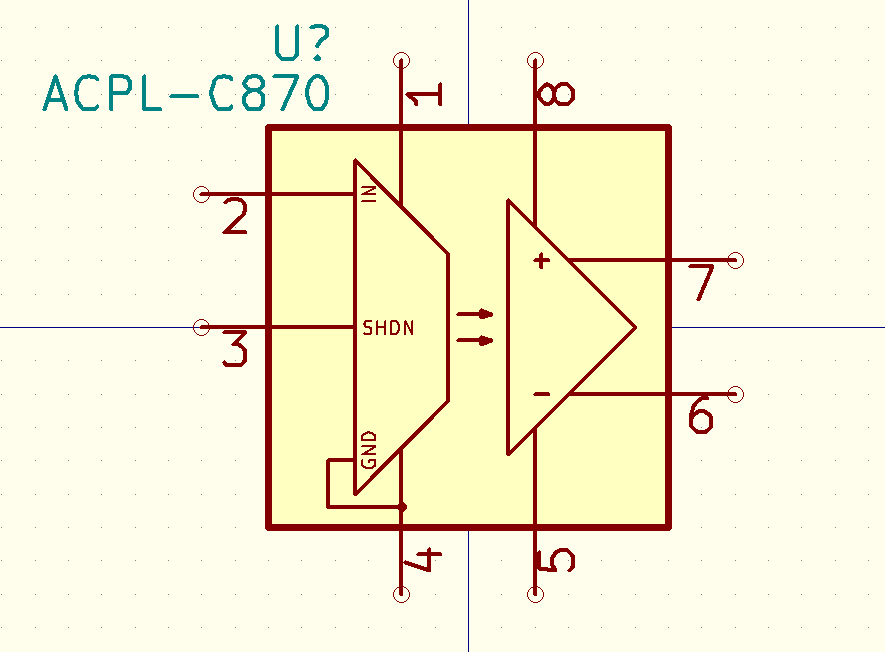
S3.4 Symbols with complex functionality may incorporate simple functional diagrams
For black box symbols with complex functionality (e.g. special function ICs), a simplified diagram of the symbol functionality may be drawn on the symbol. This may be used to provide functional clarity in a schematic.
-
Functional drawing must remain simple
-
Do not add functional drawings for multi-function components (e.g. microcontrollers)
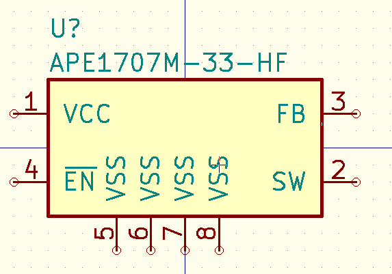
S3.5 Pin connection points must be placed outside of the symbol
Connection points for symbol pins must be placed outside the symbol body and must not require a connecting wire to cross the symbol.
Example of incorrect symbol:
Example of correct symbols:
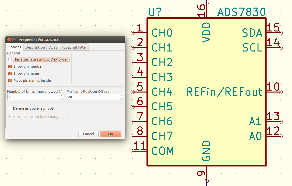
S3.6 Pin name position offset
-
Pin name position offset must not exceed
50mil(1.27mm) -
Pin name position offset should not be set less than
20mil(0.508mm) -
Preferred value is
20mil -
Larger offset allowed to accomodate particular symbol geometry
Examples:
S3.7 Pin numbering for specialized pads
For IC components with exposed pads, the number of the exposed pad should start one greater than the pin-count of the footprint.
For a SOIC-8 package with a single exposed pad, the exposed pad will be assigned the number 9
Shielded components use "SH" as the pin number for connecting the shield. For a pin to qualify as the shield pin it must be connected to a metal enclosure. For connectors it must connect to the shield of the cable.
Parts that include mechanical mounting pads without electrical use, get the pin number "MP". Non plated through holes do not get any pad number assigned. (They do not get a pin in the symbol.) An example for such a pure mechanical mounting pad would be the pads for the two metal leads on the side of Molex picoblade smd connectors.
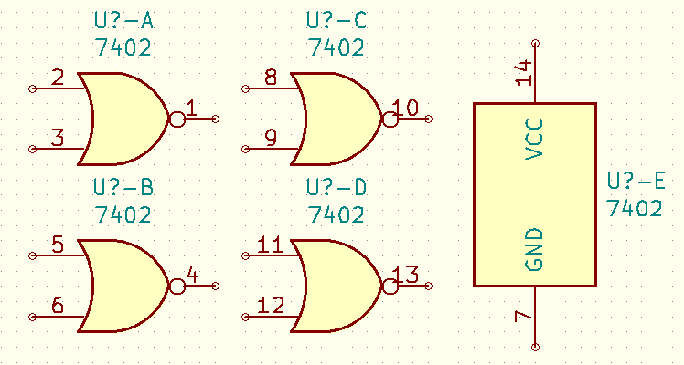
S3.8 Multi unit symbols
-
For symbols with multiple units that are drawn separately, where the units share common power pins, a separate unit should be drawn which contains these power pins.
This approach should not be taken for single-unit symbols. Power pins in this case must be drawn on the same symbol as the logic pins.
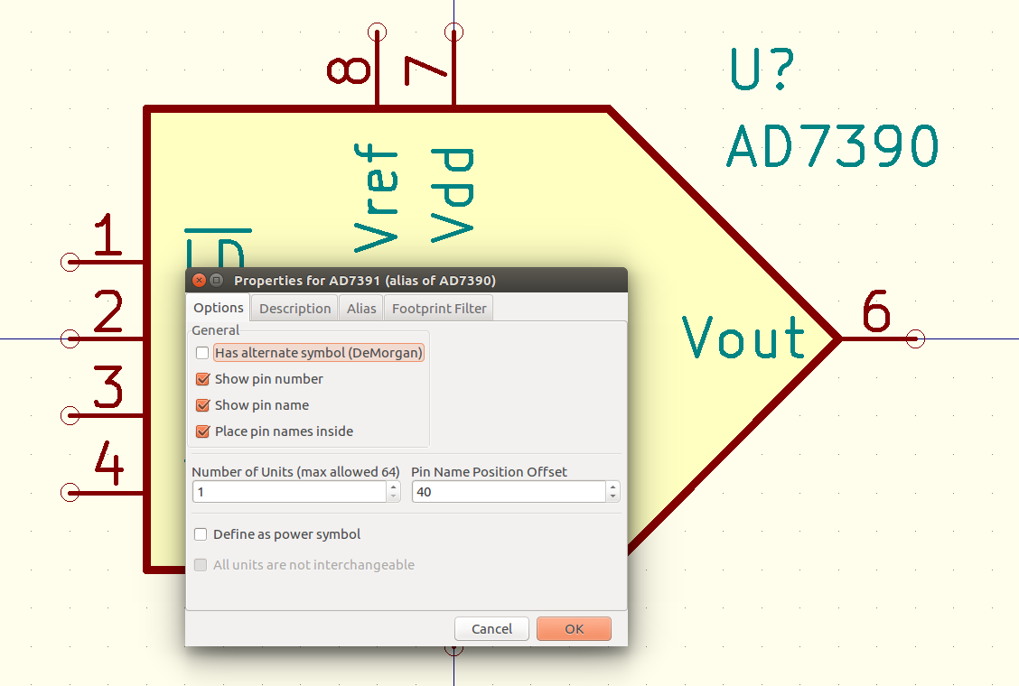
S3.9 De-Morgan representation
A symbol should not have an alternate body style. The De Morgan representation feature should not be used.
S4 - Pin Requirements
S4.1 General pin requirements
-
Using a
100mil(2.54mm) grid, pin origin must lie on a grid node (IEC-60617) -
Pins should have a length of at least
100mil(2.54mm)-
Pin length can be increased in steps of
50mil(1.27mm) -
The number of characters in the pin number determine a pin’s length. When there are two characters in the pin number then
100mil(2.54mm) long pins should be used, when three characters then150mil(3.81mm) long pins should be used, etc. -
Pin length must not exceed
300mil(7.62mm) -
Shorter pins are allowed on simple symbols for discrete devices such as resistors, capacitors, etc.
-
All pins on a symbol must have the same length
-
-
Pin numbers must be unique (no two pins may have the same number)
-
Pin names should match the pin names as specified in datasheet
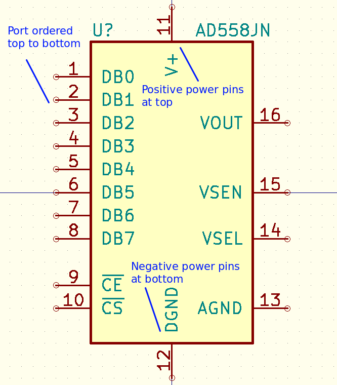
S4.2 Pins should be grouped by function
Where possible, pins should be grouped by similar function, rather than by their physical location on the associated footprint. This provides cleaner schematic routing and symbols are easier to understand in the schematic.
-
Pins with similar functions should be grouped together:
-
SPI_MISO,SPI_MOSI,SPI_CS,SPI_CLK -
UART_TX,UART_RX
-
-
Ports should be ordered from top to bottom
-
Positive power pins should be placed at the top of a symbol
-
Vcc,Vdd,Vin,V+, etc.
-
-
Negative power and ground pins should be placed at the bottom of a symbol
-
GND,Vss,V-, etc. -
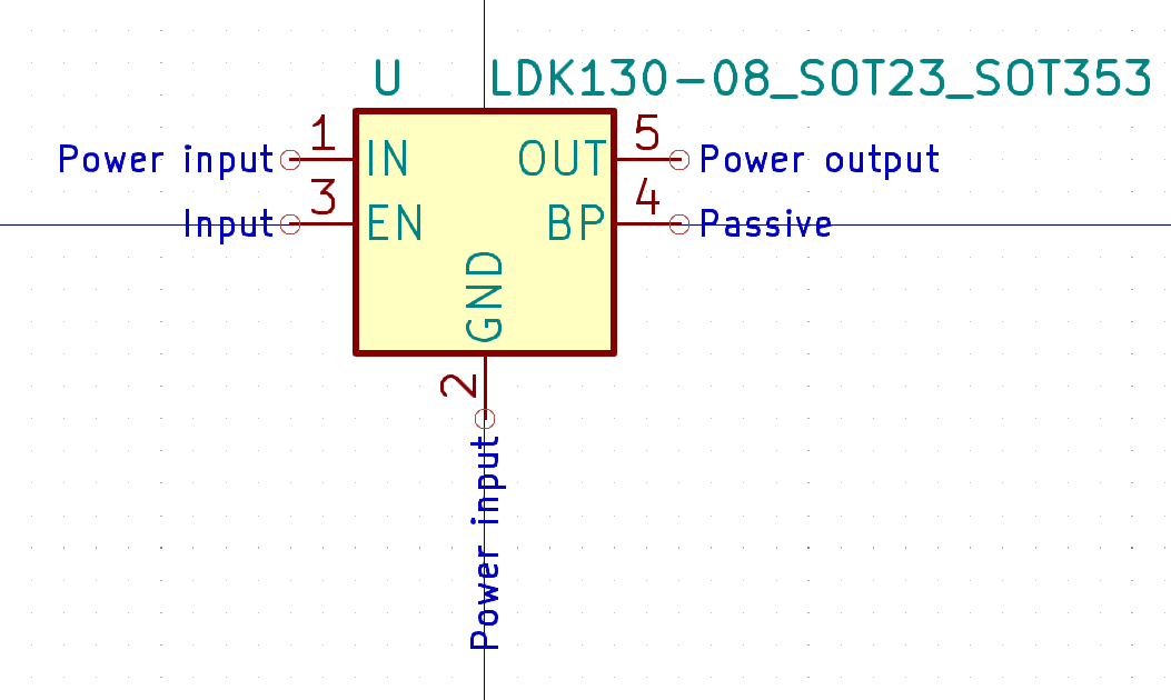
Exception Devices intended for power conversion that have both a power in- and output should have the power input pins on the left and the power output pins on the right.
-
-
Input/Control/Logic pins should be placed on the left of a symbol
-
Enable,Sleep -
Iset
-
-
Output/Controlled/Driver pins should be placed on the right of a symbol
-
Alarm -
ChargeFinished -
Q,!Q
-
-
Bus connections like SPI/I²C/.. should be arranged according to library standards (Examples can be found in the wiki, https://gitlab.com/groups/kicad/libraries/-/wikis/Symbole-Bus-Pin-Order)
S4.3 Rules for pin stacking
Many symbols have corresponding footprints where multiple physical pins are connected to a single logical net. It is desirable that in such cases the user only has to connect a single pin in the schematic, and it will automatically route to all the physical pins on the PCB. (This is not only done to reduce clutter in the schematic drawing. The main reason is to move some responsibility for correct connections from the circuit designer over to the library.)
KiCad currently has no native method for designating that a particular symbol pin maps to multiple footprint pins. The following guide serves as a workaround for designing such symbols.
In the schematic view, pins that share the same position are considered to be connected by the KiCad routing algorithm. Thus, pins can only be placed in the same location under a very specific set of circumstances:
-
Pins must not be of type
No Connect(these pins should never be connected together) -
Power supply pins must be stacked unless the datasheet specifies the need for decoupling capacitors on every pin.
-
Pins are logically connected in the symbol
-
Pins must have the same name
-
Pins must have the same electrical type
-
One pin in the stack must be visible (all other pins set to invisible)
Special Case: Pins of electrical type [Output, Power Output, Power Input] are special cases.
-
Connecting
OutputorPower Outputpins would result in an ERC error. Output pins that always need to be connected together must therefore be stacked. The invisible pins get the pin typepassivein this case. -
Invisible
Power Inputpins are global labels. This is to be avoided. For this reason the electrical typepassiveis to be used for the invisible pins in such stacks.
S4.4 Pin electrical type
Pin Electrical type should be set to match the appropriate pin function
-
Power and ground pins should be set to either
Power InputorPower Output -
Logic pins should be set according to datasheet requirements
-
Pins with programmable functionality (e.g. MCU I/O ports) should be set to
Bidirectional -
Pins must not be 'double inverted' by assigning the inverting graphical symbol and also having a bar above the name of the pin
S4.5 Pins not connected on the footprint may be omitted from the symbol
Often a component has pins that are not physically connected. Even these pins should be included in the symbol. Refer to the requirements for hidden pins.
However in some cases unconnected pins may be omitted from the schematic symbol.
-
Pins may only be omitted if they are never to be connected under any circumstances
-
Unconnected pins may only be omitted if including them would make the symbol unnecessarily large.
-
If pins are designated
NCbut the datasheet specifies that these must be pulled to ground or otherwise connected to a specific net, then these must be shown on the schematic symbol -
The footprint filter must include the pad count of the footprint if the symbol has omitted pins (see also requirements for footprint filters)
-
BGA?144 -
QFN?20
-
S4.6 Hidden pins
Hidden symbol pins are generally not allowed for schematic symbols. Any connection point must be visible, otherwise unexpected net connections can occur.
Exceptions
-
Power input pins must not be invisible unless used in power symbols (hidden power input pins are global labels). Refer to the requirements for pin stacking
-
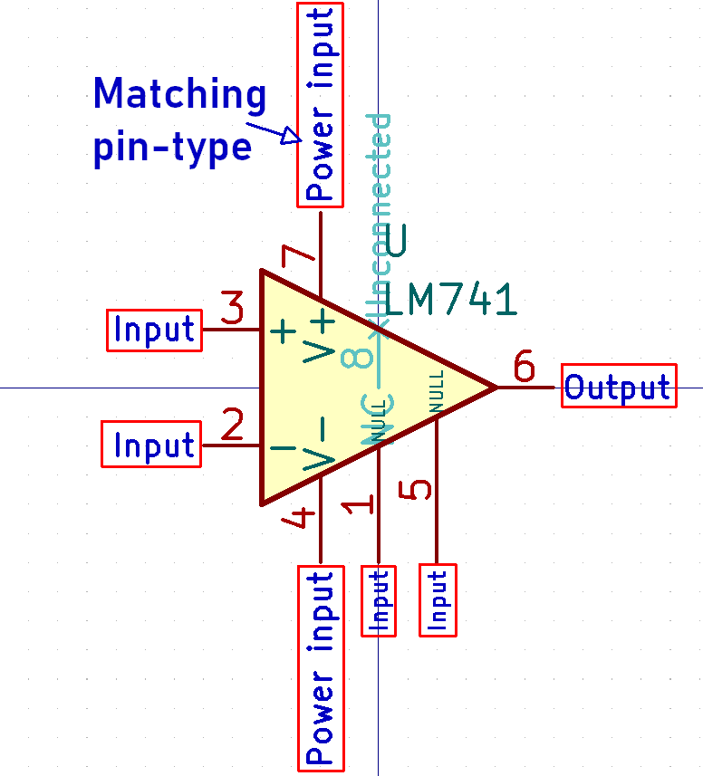
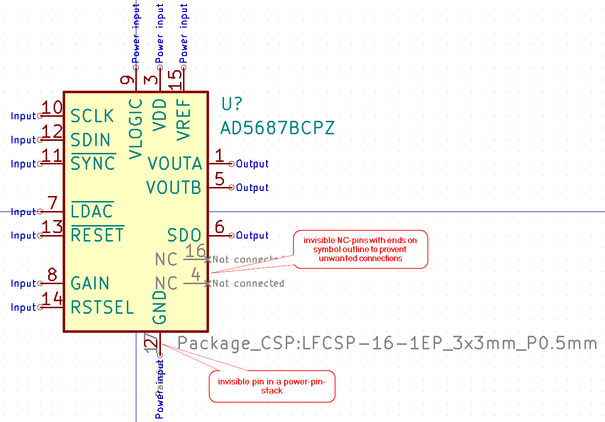
Pins that are not intended to be connected must be set to invisible. In this case the electrical type must be
Not Connected. The end of the pin should lie within or on the symbols outline to prevent unwanted connections to the invisible pin (see screenshot below).-
Pins specified as not connected may be shown if they are expected to be connected in a significant number of usecases. (Example: The datasheet suggests them to be connected to ground or some other potential for better EMC behaviour.)
-
-
Invisible pins may be used in a pin stack to allow one-to-many connections. Refer to the requirements for pin stacking
S4.7 Active low pins should be designated using a bar above the symbol name
Rather than selecting the active low graphical pin style, active low pins should be designated using a bar above the pin name.
This provides a cleaner look for the schematic.
To place a line above the pin text, add curly brackets {} around the name, and prefix with the (~) character. In case of a pin name where only a part of it is
active low, and hence, not all of it needs a bar above, e.g. \~{SPD_LED}/GPIO2.
If the pin name given by the manufacturer includes an active low prefix or suffix, it should be removed when adding the bar above it
to avoid negating it twice. For example for nRESET, use ~{RESET}.
S5 - Footprint Association
S5.1 Symbols with a default footprint link to a valid footprint file
-
For atomic symbols (those with an associated default footprint), the Footprint field must be filled with a valid entry of the format
<footprint_library>:<footprint_name>. -
For generic symbols (those which map to multiple possible footprints), the Footprint field must be left blank
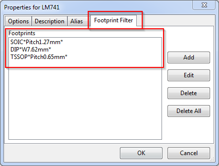
S5.2 Footprint filters must match all appropriate footprints. They should be designed to result in no false suggestions.
Footprint filters are used to help match appropriate footprints to a given symbol. This is important even for fully specified symbols (symbols with only one matching footprint), as there still may be multiple compatible footprints with different variants or options (e.g. _HandSoldering, _Heatsink, _ThermalVias).
Footprint filters use wildcard pattern matching, and allow the following wildcards:
-
*- Match zero or many characters -
?- Match zero or one characters
The library name can be used as a filter criterium. The delimiter between library and footprint filtering is :
Filter conventions:
-
Filters must end with a
*wildcard to allow matching of modified footprint suffixes -
Filters must match the dimensional information (where required) to be as specific as necessary:
-
DIP*W7.62mm*to matchDIP-22_W7.62mmbut notDIP-22_W9.3mm -
The size of the mask cutout is not included in the filter.
-
Exposed/thermal pad sizes are included in the filter if that is necessary to distinguish between otherwise-ambiguous footprints.
-
-
Filters must not contain the pin count if the pin-count in the symbol matches the pin count in the footprint. In those cases the footprint is matched by KiCad’s pin count filter. If not all pins are present in the symbol (e.g. NC-pins) the pin-count has to be part of the footprint filter (see requirements for NC pins). Then e.g.
SOT?23?5might be used instead of simplySOT?23*to matchSOT-23-5.-
Special pin specifiers are always included. Meaning the specifier for Exposed pads
EP, Mounting padMPand ShieldSHincluding their count must be included if the symbol uses these pins. (Filter for QFN-16-1EP_3x3mm_P0.5mm_EP1.8x1.8mm would beQFN*1EP*3x3mm*P0.5mm*)
-
-
By default, the footprint search does not include the name of the footprint library. To force the library name to be included, add the
:(colon) character to the filter. Text appearing before the:will match the library name. Text appearing after the:will match the footprint name.-
Connector*:*Pitch?1.25mm*will match any footprint with '1.25mm' pitch, only in libraries that begin with the text 'Connector'
-
-
Escape the characters
-and_by replacing them with?.-
SOT?23will matchSOT-23andSOT_23. This gives more flexibility in matching footprint naming.
-
Footprint filters can be set in the Footprint Filter tab in the Symbol Properties window.
S6 - Symbol Metadata
S6.1 Component Reference Designator (RefDes)
The symbol Reference Designator must be filled out appropriately for the particular type of symbol.
The table below provides a list of appropriate RefDes values. If you do not find an appropriate component entry, consult with the KiCad library team.
| Designator | Component Type |
|---|---|
| A | Sub-assembly or plug-in module |
| AE | Antenna |
| BT | Battery |
| C | Capacitor |
| D | Diode |
| DS | Display |
| F | Fuse |
| FB | Ferrite bead |
| FD | Fiducial |
| FL | Filter |
| H | Hardware (mounting screws, etc) |
| J | Jack, fixed part of a connector pair |
| JP | Jumper / link |
| K | Relay |
| L | Inductor, coil, ferrite bead |
| LS | Loudspeaker or buzzer |
| M | Motor |
| MK | Microphone |
| P | Plug, movable part of a connector pair |
| Q | Transistor |
| R | Resistor |
| RN | Resistor network |
| RT | Thermistor |
| RV | Varistor |
| SW | Switch |
| T | Transformer |
| TC | Thermocouple |
| TP | Test point |
| U | Integrated circuit (IC) |
| Y | Crystal / oscillator |
| Z | Zener diode |
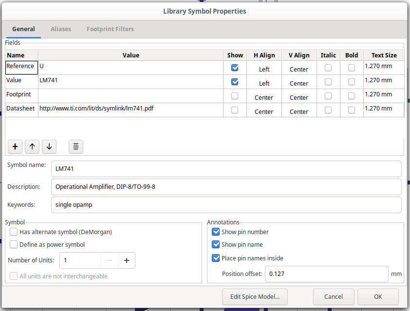
S6.2 Symbol fields and metadata filled out as required
-
Reference field is selected appropriately for the symbol and is visible
-
Value field contains the name of the symbol and is visible
-
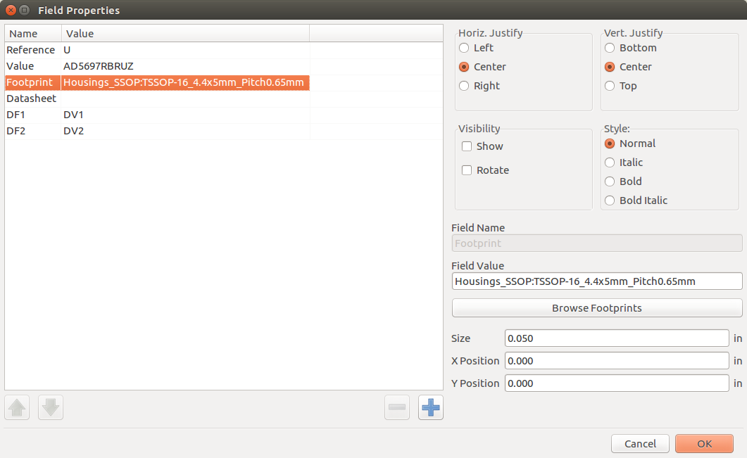
Footprint field contains footprint link for fully specified symbols and must be invisible
-
The footprint field must be empty for generic symbols
-
-
Datasheet entry is filled out, and is invisible
-
For generic symbols, the datasheet field should be a tilde (
~)
-
-
KLC Exception properties are allowed start with "KLC_" and are allowed, but they should only be added after a discussion with a librarian.
-
The symbol contains no other custom fields
Additional documentation is provided via two other fields:
-
Description field contains comma-separated device information
-
For symbols with a default footprint, the simplified footprint name should be appended to the description e.g.
SOIC-8 -
Part name should not be duplicated in the description field
-
-
Keywords field contains space-separated keyword values. These values are used to assist in part searching and should be selected to assist end-users in finding suitable parts
-
Keywords should contain typical aliases for words, Example: Description contains
Operational amplifier⇒ keywords should containopamp. -
Keywords should not include filler words. Example
positive negativeinstead ofpositive and negative -
Any single word which already appears in the description field, should not be included in the keywords field. Example: Description =
50mA Low-Dropout voltage regulator, QFN-16⇒ Keywords could includeLDObut notregulatororQFN -
In case phrases (multiple words which belong together) are used in the keywords, the must not be separated by spaces, but by a dash. Example:
voltage-regulatorinstead ofvoltage regulator -
Words which are prefixes of other words from either the Keywords or Description field should not appear in the keywords. Example: Description =
FPGA with Brown-Out detection, QFN-16⇒ Keywords could includebrownoutbut notbrown
-
S7 - Special Symbols
S7.1 Power symbols
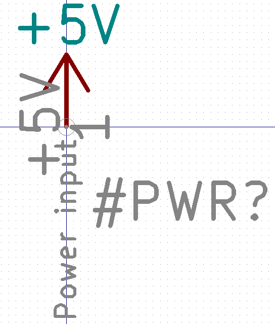
Power symbols are special symbols in KiCad, used to designate global nets for power connections.
-
Reference Designator must be set to
#PWR -
Power symbols must contain exactly one pin, which is set to visible. Note: Before KiCad 8, power symbol pins needed to be invisible, but in KiCad 8 and later they should be visible
-
Electrical pin type must be set to
Power Input -
Pin name must be set to
~ -
Value field must match the symbol name
-
Checkbox
Define as power symbolmust be checked
The example image below demonstrates the requirements as listed above:
S7.2 Graphical symbols
Graphical symbols represent "drawing" rather than physical components. They may or may not correspond to an object on the PCB.
For all graphical symbols:
-
Symbol name must be set to invisible
-
Graphical symbols must not contain any pins
-
The option
exclude from BOMmust be checked
For symbols that may appear on a PCB (e.g. an OSHW logo), the default is to set them up such that a footprint can easily be assigned:
-
Reference Designator must be set to
SYMand must be visible -
Most graphical symbols match multiple footprints (e.g. different sizes, layers or styles).
-
Set footprint filters appropriately
-
Only add a default footprint if there is unambiguously only one possible suitable footprint.
-
-
The option
exclude from boardmust not be set
For symbols that will never appear on the PCB:
-
Reference Designator must be set to
#SYMand must be invisible -
The option
exclude from boardmust be checked
Example of a symbol which may have a footprint:
Example of a symbol which will never have a footprint:
Footprint Guidelines
The following guidelines apply to PCB footprints and footprint libraries.
F1 - Footprint Libraries
F1.1 Footprint libraries are categorized by function
Footprints are grouped into libraries (directories with .pretty extension) based on their primary function. As an extension of this, footprint libraries should be named based on this same functionality.
Library names must be defined based on the priority list below, with each element separated by the underscore (_) character:
-
Function (e.g.
Conn,Capacitor) -
Sub-function (e.g.
HDMI,USB) -
Tertiary qualifier (e.g.
RightAngle,SMD) -
Manufacturer name (e.g.
Texas,Microchip) -
Footprint series name (e.g.
MicroFit) -
Extra library descriptors as required
Note: Some of the elements listed above may be omitted if not required.
Example footprint library names:
-
Conn_USB_SMD- Surface mount USB connectors -
Conn_Molex_MicroFit- Molex MicroFit series rectangular connectors -
Capacitor_Tantalum_SMD- Surface mount Tantalum capacitors
F1.2 Connector footprint libraries
Categorizing connectors by function can prove difficult as many connectors can be used in a wide variety of applications.
Therefore, categorization of connector footprints is given special consideration as detailed below:
-
Connectors are grouped firstly by their primary function (where such a function exists). Examples of primary function include:
-
Conn_USB -
Conn_HDMI -
Conn_Ethernet
-
-
When primary function libraries become too large, they can be split by sub-function or by manufacturer
-
Conn_USB_Molex -
Conn_DSUB_HighDensity
-
-
For connectors without a specific function, then connectors are grouped by their mechanical type:
-
Conn_Barrel -
Conn_DIN -
Conn_DSUB -
Conn_PinHeader -
Conn_PinSocket -
Conn_Rectangular
-
-
Connector libraries can be further split by another qualifier:
-
Conn_PinHeader_2.54mm -
Conn_PinHeader_1.27mm
-
-
Connector libraries can also be split by manufacturer and series, for multi-purpose connectors
-
TerminalBlock_Phoenix_MKDS -
TerminalBlock_Phoenix_PT -
TerminalBlock_Wago -
Conn_JST -
Conn_Hirose_DF13
-
F2 - General Footprint Naming Guidelines
F2.1 General footprint naming conventions
Each footprint is a .kicad_mod file (stored within a .pretty directory). The naming convention for a given footprint depends largely on the type of footprint, however a general guide is presented below:
-
Specific package type is written first, e.g.
-
QFN- Quad Flat No-Lead package -
C- Capacitor
-
-
Package name and number of pins are separated by a hyphen
-
TO-90 -
QFN-48 -
DIP-20
-
-
Packages with special pads add an identifier to the pin count field separated by a hyphen
-
The field includes the count of uniquely numbered pads of this type.
-
For exposed pads (large copper pad below the part)
[count]EP -
For shield pads
[count]SH(Unless such a pin is already expected for the part. An example would be a HDMI connector.) -
For pads connecting pure mechanical mounting leads
[count]MP
-
-
Examples from the library.
-
DFN-6-1EP_2x2mm_P0.5mm_EP0.61x1.42mm -
Samtec_LSHM-110-xx.x-x-DV-S_2x10-1SH_P0.50mm_Vertical -
Molex_PicoBlade_53261-0271_1x02-1MP_P1.25mm_Horizontal
-
-
-
Unique fields (parameters) in the footprint name are separated by
_character. -
Package dimensions are specified as
lengthxwidth(and optionallyheight)-
3.5x3.5x0.2mm -
1x1in -
If necessary for clarity, footprint body dimensions may be prefixed with a leading
B
-
-
Pin layout
-
1x10 -
2x15
-
-
Pitch is specified with a leading
P:-
P1.27mm- 1.27mm pitch -
P5.0mm- 5.0mm pitch
-
-
Modifiers to standard footprint values
-
Drill1.25mm -
Pad2.4x5.2mm
-
-
Orientation e.g.
Horizontal,Vertical -
Any modification to the original footprint, indicated by appending the reason
-
_HandSoldering -
_ThermalVias -
_CircularHoles
-
Not all of the fields defined above are strictly required for a particular footprint. Additional fields may also be added as needed.
F2.2 Footprint naming field prefixes
A footprint name has to convey a lot of information to clearly specify the purpose and parameters of the footprint. Some fields in footprint names are common to many footprints and can be shortened using special abbreviations.
Not all footprints will require the use of these abbreviations - they are provided as a method of standardising the manner in which footprint parameters are called out when encountered.
In many cases, the major dimensions (x/y/z) of a footprint may be specified without a prefix, as the body dimensions are assumed to have the greatest priority in the footprint name. Therefore, the "3.2x5.7mm" part of the example name below requires no 'B' prefix, and is not required to be written as "B3.2x5.7mm".
e.g. SOIC-8_3.2x5.7mm_P1.27mm
In cases where potential conflicts exist, however, the body dimensions must be explicitly named with the prefix B.
Refer to the table below for accepted prefix abbreviations.
| Prefix | Field Description | Notes |
|---|---|---|
| B | Body dimensions |
|
| D | Diameter |
|
| H | Height |
|
| L | Length |
|
| O | Offset |
|
| W | Width |
|
| EP | Exposed pad dimensions |
|
| P | Pad pitch |
|
| T | Thickness | Component thickness, where appropriate |
Examples:
-
LQFP-32_4x4x1.1mm_P1.65mm- LQFP package, 32 pins, 4x4mm body, 1.1mm height, 1.65mm pitch -
CP_Radial_D4.5mm_P2.5mm_H10mm- Radial polarized capacitor, 4.5mm diameter, 2.5mm pitch, 10mm height
If the parameter is not found in the table above, the name of the parameter should be entered in full.
Following is a list of examples of (non-abbreviated) parameter names used in footprint naming
| Prefix | Field Description |
|---|---|
| Ball | BGA Ball diameter |
| Clearance | Clearance between pin rows |
| Drill | Drill diameter |
| Layout | Specific footprint layout e.g. Layout3x7 for a BGA with 21 balls arranged in 3 columns and 7 rows |
| Lead | Lead dimensions |
| Mask | Custom soldermask dimensions |
| Pad | Custom pad dimensions |
| Tab | Tab dimensions |
F2.3 Manufacturer specific version of generic footprints
If a manufacturer footprint deviates from the "standard" footprints available, then this should be added to the library and designated as manufacturer-specific.
-
If a footprint is specific to a single manufacturer, this must be indicated by prepending the manufacturer name and MPN to the footprint name.
-
Texas_S-PVQFN-N48_
-
-
Sometimes the component datasheet will have specific requirements which do not conform to KLC requirements. A common example is specific requirements for the shape of stencil (solder paste layer).
In such cases, the KLC requirements can be superseded by the datasheet requirements, at the discretion of the KiCad library team.
F2.4 Footprint naming for non-standard pin numbering
Generally, a footprint should include a field of the format <pkg>-<pincount>, e.g.
-
SOIC-8 -
QFN-24
In the majority of cases, the pin quantity is self explanatory and is sufficient to describe the number of pins on the symbol.
However there may be cases where this numbering is insufficient. Where the number of footprint pins does not match the number of package pins, exceptions must be made.
Exception: Omitted pins, missing pin numbers are skipped
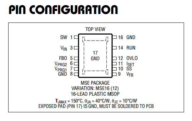
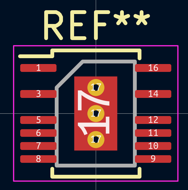
Example: LTC3638
The LTC3638 comes in an MSOP-16 package which has four missing pins, for increased voltage isolation.
In this case, the numbers for the missing pins are skipped and the normal pin numbers are assigned to the remaining pins.
To indicate this, the footprint should be named as follows:
PKG-<xx>-<yy> where:
-
xx= number of remaining pins -
yy= number of remaining pins + number of removed pins
In the LTC3638 example above, this would result in:
MSOP-12-16
The footprint pads should be numbered like so:
F2.5 Footprint naming conventions for specific components
Footprint naming is sufficiently complex that a general rule is not enough to fully define a naming scheme that fits the wide range of footprints.
F3 - Specific Footprint Naming Guidelines
F3.1 SMD chip package naming conventions
The following footprint naming conventions should be used as examples for naming SMD chip package footprints.
If you do not find an appropriate convention that matches a particular footprint type, either contact the KiCad library team or try to match a convention set by existing library components.
In the entries below, variable fields are denoted as follows:
- Fixed fields
- Mandatory fields
- Optional fields
- Prefix - Device type
- Imperial size - Imperial case size (Optional)
- Metric size - Metric case size (Optional)
- Modifiers - Modifiers to footprint if non standard (Optional)
- Options - Extra footprint options (Optional)
Example:
Notes:
The prefix is determined by the default reference designator of the device, e.g.
-
Capacitor =
C -
Capacitor (polarised) =
CP -
Resistor =
R -
Diode =
D
Case size codes:
| Imperial Code | Metric Code | Size Imperial | Size Metric |
|---|---|---|---|
01005 |
0402 |
0.0157 in × 0.0079 in |
0.4 mm × 0.2 mm |
0201 |
0603 |
0.024 in × 0.012 in |
0.6 mm × 0.3 mm |
0402 |
1005 |
0.039 in × 0.020 in |
1.0 mm × 0.5 mm |
0603 |
1608 |
0.063 in × 0.031 in |
1.6 mm × 0.8 mm |
0805 |
2012 |
0.079 in × 0.049 in |
2.0 mm × 1.25 mm |
1008 |
2520 |
0.098 in × 0.079 in |
2.5 mm × 2.0 mm |
1206 |
3216 |
0.126 in × 0.063 in |
3.2 mm × 1.6 mm |
1210 |
3225 |
0.126 in × 0.098 in |
3.2 mm × 2.5 mm |
1806 |
4516 |
0.177 in × 0.063 in |
4.5 mm × 1.6 mm |
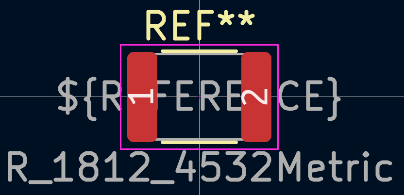
1812 |
4532 |
0.18 in × 0.13 in |
4.5 mm × 3.2 mm |
1825 |
4564 |
0.18 in × 0.25 in |
4.5 mm × 6.4 mm |
2010 |
5025 |
0.197 in × 0.098 in |
5.0 mm × 2.5 mm |
2512 |
6332 |
0.25 in × 0.13 in |
6.3 mm × 3.2 mm |
2920 |
7451 |
0.29 in × 0.20 in |
7.4 mm × 5.1 mm |
F3.2 Resistor naming conventions
The following footprint naming conventions should be used as examples for naming resistor footprints.
If you do not find an appropriate convention that matches a particular footprint type, either contact the KiCad library team or try to match a convention set by existing library components.
In the entries below, variable fields are denoted as follows:
- Fixed fields
- Mandatory fields
- Optional fields
Axial Resistors
- Length - Resistor body length
- Diameter - Body diameter
- Pitch - Lead spacing
- Modifiers - Modifiers to footprint specifications (Optional)
- Orientation - Resistor orientation (Vertical / Horizontal) (Optional)
- Options - Extra footprint options (Optional)
Example:
F3.3 Capacitor naming conventions
The following footprint naming conventions should be used as examples for naming capacitor footprints.
If you do not find an appropriate convention that matches a particular footprint type, either contact the KiCad library team or try to match a convention set by existing library components.
In the entries below, variable fields are denoted as follows:
- Fixed fields
- Mandatory fields
- Optional fields
SMD Chip Capacitor
- C/CP - Capacitor style (polarised or non-polarised)
- Imperial size - Imperial case size (Optional)
- Metric size - Metric case size (Optional)
- Modifiers - Footprint modifiers if non standard (Optional)
- Options - Footprint options (Optional)
Example:
Notes:
-
At least one case size (either imperial or metric) must be specified
-
Metric case size must have the suffix
Metric
SMD Tantalum Capacitor
- Metric size - EIA metric size code
- Size code - Letter size code including naming standard ([Standard]-[Letter])
- Modifiers - Footprint modifiers if non standard (Optional)
- Options - Footprint options (Optional)
Example:
| EIA Metric size | Body size (XxYxZ) | Kemet Code | AVX Code |
|---|---|---|---|
1608-08 |
1,6 x 0,8 x 0,8 mm |
— |
J |
1608-10 |
1,6 x 0,85 x 1,05 mm |
— |
L |
2012-12 |
2,05 x 1,35 x 1,2 mm |
R |
R |
2012-15 |
2,05 x 1,35 x 1,5 mm |
— |
P |
3216-10 |
3,2 x 1,6 x 1,0 mm |
I |
K |
3216-12 |
3,2 x 1,6 x 1,2 mm |
S |
S |
3216-18 |
3,2 x 1,6 x 1,8 mm |
A |
A |
3528-12 |
3,5 x 2,8 x 1,2 mm |
T |
T |
3528-15 |
3,5 x 2,8 x 1,5 mm |
— |
H |
3528-21 |
3,5 x 2,8 x 2,1 mm |
B |
B |
6032-15 |
6,0 x 3,2 x 1,5 mm |
U |
W |
6032-20 |
6,0 x 3,2 x 2,0 mm |
— |
F |
6032-28 |
6,0 x 3,2 x 2,8 mm |
C |
C |
7343-15 |
7,3 x 4,3 x 1,5 mm |
W |
X |
7343-20 |
7,3 x 4,3 x 2,0 mm |
V |
Y |
7343-30 |
7,3 x 4,3 x 3,0 mm |
— |
N |
7343-31 |
7,3 x 4,3 x 3,1 mm |
D |
D |
7343-40 |
7,3 x 4,3 x 4,0 mm |
Y |
— |
7343-43 |
7,3 x 4,3 x 4,3 mm |
X |
E |
7360-38 |
7,3 x 6,0 x 3,8 mm |
E |
— |
7361-38 |
7,3 x 6,1 x 3,8 mm |
— |
V |
7361-438 |
7,3 x 6,1 x 4,3 mm |
— |
U |
SMD Electrolytic Capacitor
- Manufacturer - Manufacturer name (Optional)
- X - Case size in x dimension
- true - Case size in y dimension
- [Height] - Case height (Optional)
- [Pitch] - Lead spacing (Optional)
- [Modifiers] - Footprint modifiers if non-standard (Optional)
- [Options] - Footprint options (Optional)
Example:
THT Capacitor
- C/CP - Capacitor polarisation
- Style - Capacitor case style (see notes below)
- Case size - Body length (Optional)
- Diameter - Case diameter (Optional)
- Width - Body width (Optional)
- Pitch - Lead spacing
- Modifiers - Footprint modifiers if non-standard
- Options - Footprint options (Optional)
Example:
Notes:
-
There are different capacitor styles available:
-
Axial: Cylindrical body with axial lead attachment.
-
Radial: Cylindrical body, both leads enter at same end.
-
Disc: Disc shaped body (sometimes enclosed), leads enter tangent to the inner disc
-
Rect: Box shaped body (Bottom face in contact with the board)
-
-
Body size:
-
For Axial body styles: L[length]_D[diameter]
-
For Radial body style: D[diameter]{_H[height]}
-
For Disc body style: D[diameter]_W[width]{_H[overall height]}
-
For box shaped body styles: [X]x[Y]{x[Z]}
-
F3.4 SMD IC package naming conventions
The following footprint naming conventions should be used as examples for naming SMD IC package footprints.
If you do not find an appropriate convention that matches a particular footprint type, either contact the KiCad library team or try to match a convention set by existing library components.
In the entries below, variable fields are denoted as follows:
- Fixed fields
- Mandatory fields
- Optional fields
Gullwing Packages
The format below provides a guide for naming Gullwing IC packages.
Examples:
-
SOIC
-
SOP
-
QFP
-
J-Lead
- PKG - Package name
- Pin count - Number of (unique) pins
- EP Qty - Number of exposed pads under the device (if greater than zero) (Optional)
- X - Major dimension of part on x axis
- Y - Major dimension of part on y axis
- Z - Major dimension of part on z axis (Optional)
- Pitch - Lead pitch
- Modifiers - Footprint modifiers (Optional)
- Options - Extra footprint options (Optional)
Example:
Notes:
-
[
PKG] - refers to the name most commonly used in the industry. Generally this implies JEDEC naming but some other standard may be used as required. -
[
Pin count] - the number of uniquely numbered pads (excluding any exposed pads under the device) -
[
Modifiers] - may vary for individual IC footprint types. Includes:-
Clearance
-
Lead size
-
Pad size
-
Exposed pad size
-
Soldermask expansion
-
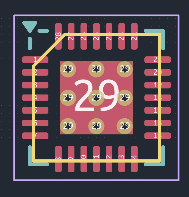
No-Lead Packages
Examples:
-
DFN
-
QFN
-
LCC
- PKG - Package name
- Pincount - Number of (unique) pins
- EP Qty - Number of exposed pads under the device (if greater than zero) (Optional)
- X - Major dimension of part on x axis
- Y - Major dimension of part on y axis
- Z - Major dimension of part on z axis (Optional)
- Pitch - Lead pitch
- Modifiers - Footprint modifiers (Optional)
- Options - Extra footprint options (Optional)
Example:
Notes:
-
The lead length is the nominal lead length for which the footprint is designed
-
Optionally the nominal lead width can also be provided
Ball Grid Array Packages
- PKG - Package name
- Pincount - Number of (unique) pins
- X - Major dimension of part on x axis
- Y - Major dimension of part on y axis
- Z - Major dimension of part on z axis (Optional)
- Columns - Number of ball columns
- Rows - Number of ball rows
- Pitch X - Ball pitch in x direction
- Pitch Y - Ball pitch in y direction (if different from x direction (Optional)
- Ball - Ball diameter
- Pad - Pad diameter
- NSMD/SMD - Solder Mask Defined or Non Solder Mask Defined
- Modifiers - Footprint modifiers (Optional)
- Options - Extra footprint options (Optional)
Example:
Notes:
-
For BGA simply providing the pin count is not sufficient. It is also necessary to provide the number of [
Columns] (x direction) and [Rows] (y direction). -
Some BGA packages have different pitch in x and y directions. If this is the case then both [
Pitch] dimensions need to be provided -
The [
Ball] diameter for which the footprint is designed needs to be provided -
[
NSMD/SMD]-
NSMD means the footprint is designed for
non solder mask defined(mask cutout is larger than copper pad) -
SMD means the footprint is designed for
solder mask defined(mask cutout is smaller than copper pad)
-
F3.5 THT IC package naming conventions
The following footprint naming conventions should be used as examples for naming THT IC package footprints.
If you do not find an appropriate convention that matches a particular footprint type, either contact the KiCad library team or try to match a convention set by existing library components.
In the entries below, variable fields are denoted as follows:
- Fixed fields
- Mandatory fields
- Optional fields
Through Hole Packages (DIP)
- PKG - Package name
- Pincount - Number of (unique) pins
- X - Major dimension of part on x axis
- Y - Major dimension of part on y axis
- Z - Major dimension of part on z axis (Optional)
- Lead span - Distance between leads
- Pitch - Lead pitch
- Modifiers - Modifiers to footprint specifications
- Options - Extra footprint options (Optional)
Example:
Notes:
-
Drill size (if specified) must be given in
mm
Through Hole Packages (TO)
- PKG - Package name
- Pincount - Number of (unique) pins
- X - Major dimension of part on x axis (Optional)
- Y - Major dimension of part on y axis (Optional)
- Z - Major dimension of part on z axis (Optional)
- Lead span - Distance between leads (Optional)
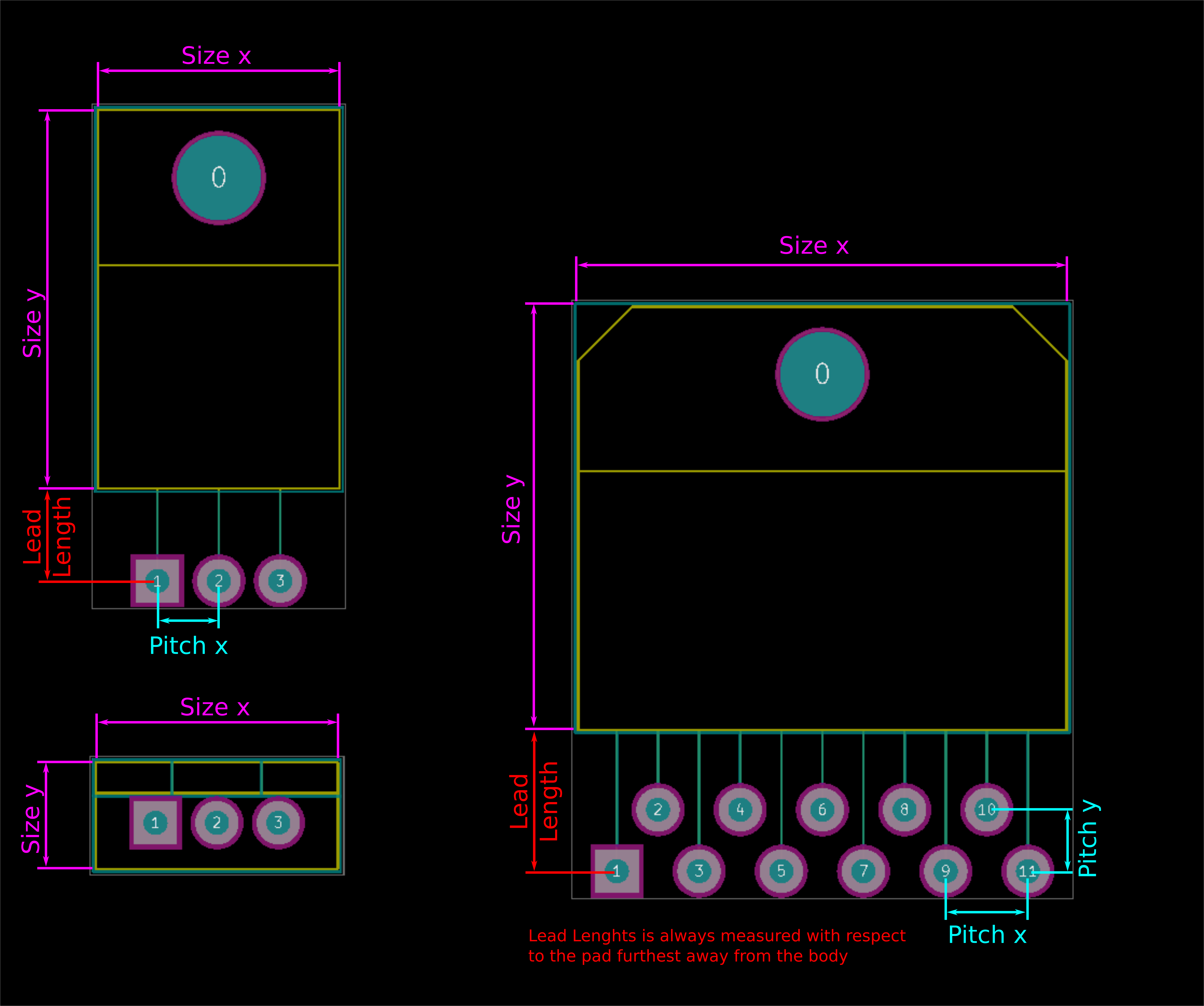
- Pitch x - Lead pitch in x dimension (Optional)
- Pitch y - Lead pitch in y dimension (if different from x dimension) (Optional)
- Stagger - Pin staggering options (Optional)
- Modifiers - Modifiers to footprint specifications (Optional)
- Orientation - Component orientation (see notes below)
- Options - Extra footprint options (Optional)
Example:
Notes:
-
Drill size (if specified) must be given in
mm -
Orientationcan be chosen from:-
Vertical
-
TabDown
-
TabUp
-
-
Staggercan be chosen from:-
StaggerOdd (odd pins are further from component body)
-
StaggerEven (even pins are further from component body)
-
Size Parameter:
Orientation:
F3.6 Connector naming conventions
The following footprint naming conventions should be used as examples for naming connector footprints.
If you do not find an appropriate convention that matches a particular footprint type, either contact the KiCad library team or try to match a convention set by existing library components.
In the entries below, variable fields are denoted as follows:
- Fixed fields
- Mandatory fields
- Optional fields
Conventions for Connectors
Connector footprints are extremely diverse and the naming conventions for connectors can be complicated. This section details some examples of naming schemes for various connector types. While there are variations between connectors, the general format for naming connectors is as follows:
- Series - Generic series name (Optional)
- Subseries - Series secondary identifier (Optional)
- Pins - Pin count (Optional)
- MPN - Manufacturer specific identifier (Optional)
- Pin layout - Pin configuration, specific to connector type (Optional)
- Pitch - Pin pitch, if not implied by connector standard (Optional)
- Modifiers - Modifiers to connector specifications (pad size, etc) (Optional)
- Orientation - Orientation of connector relative to board (Optional)
- Options - Extra footprint options (Optional)
Notes:
-
[
Series] - a versatile field which could contain:-
Functional description (e.g.
USB) -
Connector type (e.g.
PinHeaderorTerminalBlock) -
Industry standard (e.g.
DSUB-15) -
Manufacturer specific series (e.g.
Hirose_DF13)
-
-
[
MPN] (manufacturer part number) - uniquely identifies a connector according to that manufacturer’s internal naming conventions -
[
Pin layout] - dependent on the connector type-
Single row connectors: 1x[
number of pins] -
Multi row connectors with equal number of pins in each row: [
number of rows]x[number of pins per row] -
Other connectors: [
number of rows]Rows_[number of pins overall]Pins -
Connectors for standardized interfaces do not need to include the pin configuration information (e.g. USB)
-
-
Number format:
-
[
number of rows] number of rows no leading zero. -
[
number of pins per row] and [number of pins] two digit number with leading zero. (can have more digits for connectors with > 99 pins)
-
-
[
Pitch] - if the connector standard does not imply the pin pitch, then this field is required -
[
Modifiers] - multiple fields may be added here, detailing modifications or devations from the standard footprint design. Examples include:-
Pad size variation
-
Drill size variation
-
-
[
Orientation] - The orientation of the connector with reference to the board plane
-
[
Options] - Extra footprint options
In addition to these conventions, additional schemes are employed for specific connector types - these are detailed below.
Connectors for Specific Functions
Many connectors are designed for specific functions (e.g. USB, HDMI, SD-Card, etc). In these cases, specific naming conventions should be followed:
- Function - Functional purpose of the connector
- Standard - Standard to which the connector complies, if applicable (Optional)
- Size - Connector size (e.g. Micro/Mini) (Optional)
- Type - Connector sub-type (e.g. A/B/C) (Optional)
- MAN - Manufacturer name (Optional)
- MPN - Manufacturer part number (Optional)
- Modifiers - Footprint modifiers (Optional)
- Orientation - Connector orientation (Optional)
- Options - Extra footprint options (Optional)
Example:
Notes:
-
Some examples of functional connector naming are provided below:
-
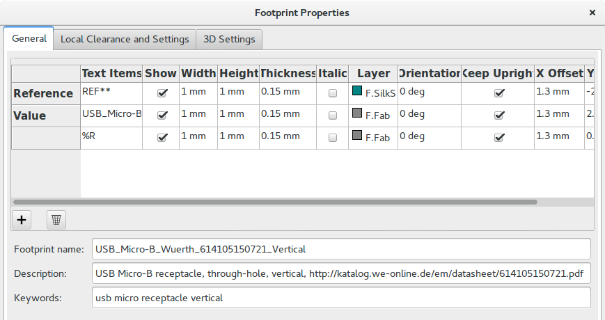
USB_Micro-B_Wuerth_614105150721_Vertical_CircularHoles -
HDMI_Micro-D_Molex_46765-2x0x -
MicroSD_Wuerth_WR-CRD_693072010801
-
-
In most cases, pin layout does not need to be explicitly specified
Connectors with Standardised Shape
Many connectors are provided by multiple manufacturers in an industry standard package or physical layout. These connectors should use the accepted industry naming at the beginning of the footprint name:
- Standard - Generic connector standard (see notes below)
- Pins - Number of pins
- Series modifier - Series Modifier (see notes below)
- MAN - Manufacturer name (Optional)
- Series - Manufacturer series name (Optional)
- MPN - Manufacturer part number (Optional)
- Pin layout - Pin configuration, if not fully defined by applicable standard (Optional)
- Pitch - Pin pitch, if not fully defined by applicable standard (Optional)
- Modifiers - Footprint modifier field(s) (Optional)
- Orientation - Connector orientation (if multiple options exist) (Optional)
- Options - Extra footprint options (Optional)
Example:
Notes:
-
The generic connector type [
Standard] defines the shape of the connector-
e.g.
DSUBTabCircular
-
Generic Connector Types
Examples of generic arrayed connectors:
-
PinHeader
-
PinSocket
-
TerminalBlock
- Connector type - Generic connector style (see notes below)
- MPN - Manufacturer specific identifier (Optional)
- Pin layout - Pin configuration layout (see notes below)
- Pitch - Pin pitch
- Modifiers - Modifiers to connector specifications (pad size, etc) (Optional)
- Orientation - Orientation of connector relative to board
- Options - Extra footprint options (Optional)
Example:
Manufacturer Specific Connectors
Manufacturer series connectors are those which are particular to a particular manufacturer standard.
- MAN - Manufacturer name (Optional)
- Series - Manufacturer series name
- MPN - Manufacturer part number
- Pin layout - Pin layout information (see notes below)
- Pitch - Pad pitch
- Modifiers - Modifiers to connector specifications (pad size, etc)
- Orientation - Direction of connector insertion relative to board plane
- Options - Extra footprint options (Optional)
Example:
Notes:
-
If the footprint is located in a library dedicated to a single manufacturer, then the
MANprefix is not required
F3.7 Fuse naming conventions
The following footprint naming conventions should be used as examples for naming fuse and fuse holder footprints.
If you do not find an appropriate convention that matches a particular footprint type, either contact the KiCad library team or try to match a convention set by existing library components.
In the entries below, variable fields are denoted as follows:
- Fixed fields
- Mandatory fields
- Optional fields
Fuse Holders
- Fuse Type - Type of fuse (Optional)
- MAN - Manufacturer name (Optional)
- Series - Manufacturer series name (Optional)
- MPN - Manufacturer part number (Optional)
- Modifiers - Footprint modifiers if non-standard (Optional)
- Orientation - Orientation of fuse, if multiple orientations are available (Optional)
- Options - Extra footprint options (Optional)
Example:
Examples of Fuse Type field:
-
Automotive fuses:
-
Automotive-Micro2
-
Automotive-Micro3
-
Automotive-LowProfile
-
Automotive-Mini
-
Automotive-ATO
-
Automotive-Maxi
-
Automotive-Bosch
-
Automotive-SFE-[SizeCode]
-
-
Industrial fuses
-
Cylinder-[diameter]x[length]mm
-
Fuses
Cylindrical Fuse
- MAN - Manufacturer name (Optional)
- Series - Manufacturer series name (Optional)
- MPN - Manufacturer part number (Optional)
- Body size - Major fuse dimensions
- Modifiers - Footprint modifiers if non standard (Optional)
- Orientation - Orientation of fuse, if multiple orientations are available (Optional)
- Options - Extra footprint options (Optional)
Example:
Rectangular SMD Fuses
- Imperial size - Imperial case size (Optional)
- Metric size - Metric case size (Optional)
- Modifiers - Footprint modifiers if non standard (Optional)
- Orientation - Orientation with respect to board plane (Optional)
- Options - Footprint options (Optional)
Example:
F4 - General Footprint Requirements
F4.1 Datasheet recommendations take priority
Where conflict exists between datasheet recommendations and KLC requirements, then (in the general case) the datasheet should take priority.
It is important when designing footprints that they adhere to requirements for soldering and assembly - often these requirements have very small tolerance for variation.
If the KLC is at odds with the datasheet, follow the datasheet, and note this difference to the KiCad library team when submitting your contribution.
F4.2 Pin 1 should be located at the top left
Footprints should be oriented such that Pin 1 is located in the upper left corner (IPC-7351).
Exceptions
Where footprints cannot be oriented with pin 1 in the top-left quadrant, pin 1 should be aligned to the top
Two-terminal footprints should be aligned with pin 1 on the left side
Multi-purpose connector footprints should be oriented horizontally, with pin 1 on the left side, for easier comparison and alignment with the matching connector.
F4.3 Connected copper elements have the same pad number
Footprints that contain multiple pads or conductive elements that are physically connected require special attention:
-
Multiple pads that are physically connected must share the same number
-
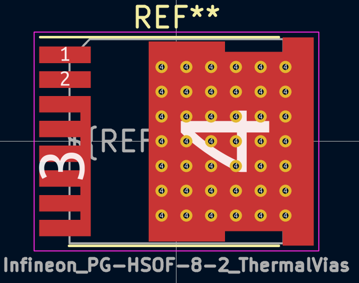
Thermal vias (if present) must share the same number as the thermal pad to which they are connected
F4.4 Thermal pads
Manufacturer datasheets may specify that thermal vias should be added to the thermal pad under a device package, to assist in moving heat away from the device.
In such cases the datasheet will usually specify the quantity, size and position of these vias.
In addition to manufacturer requirements, a number of extra conventions should be followed when creating thermal vias.
-
Thermal vias must share the same pad number as the pad on which they are placed
-
Where thermal vias are connected to a pad on the
F.Culayer, a copper pad on theB.Culayer should be added, to provide thermal relief for the via.B.Maskis not to be enabled on theB.Cupad so mask is present. This pad must be large enough to fully surround the via(s) with a margin of>= 0.5mm. Note: If the datasheet gives conflicting advice to the placement of this pad on theB.Culayer, then the datasheet instruction should be given preference.
-
Unless instructed by the datasheet, solder paste must not be placed over thermal via(s) sized 0.3mm or larger. This can cause solder to wick into the via during reflow, and cause solder joint issues.
-
When submitting a footprint with thermal vias, the suffix
_ThermalViasshould be added to the footprint name -
If it does not already exist, a second version of the footprint without the thermal vias should be added. Note: This second version should not have the
_ThermalViassuffix in the footprint name. -
The hole size should be 0.2mm - 0.3mm, unless the datasheet specifies otherwise. Note: While 0.3mm is manufacturable using lowest cost processes, 0.2 is better for reflow and no longer that expensive to manufacture, so 0.2mm is preferred for smaller parts.__
F4.5 Specifying footprint keepout areas
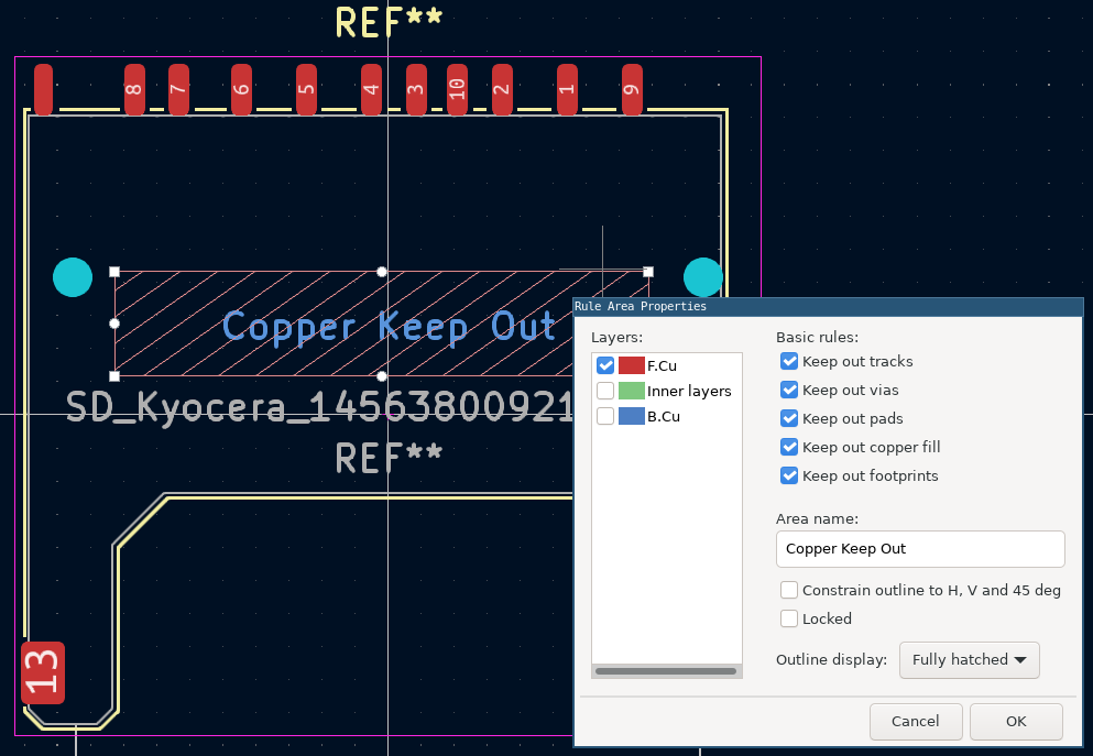
Footprint keepout area must be drawn using as a 'rule-area (keepout)' when necessary or recommended in manufacturer’s datasheet.
The area should be named according to its use (e.g. 'Antenna Keepout'), this name must be used to name the area as text also on the User.Comments layer.
-
Select only the appropriate layers
-
Check all basic rules (
Constrain outlineandLockedmust be kept unchecked) -
Outline display must be
Fully hatched
Example:
Example of an area, named both in the dialog and on the User.Comments layer:
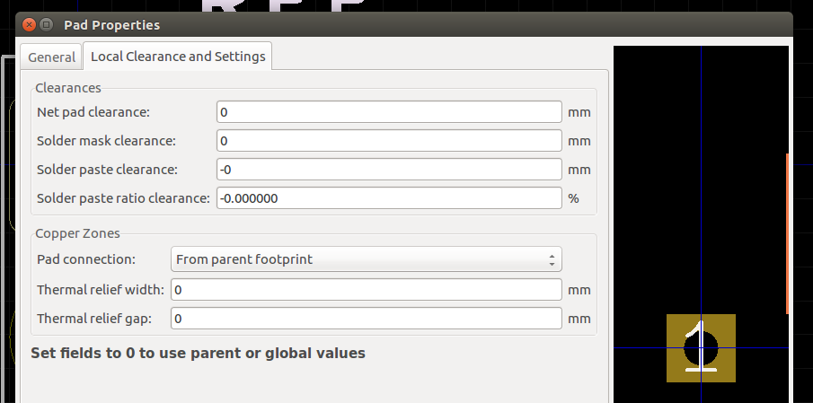
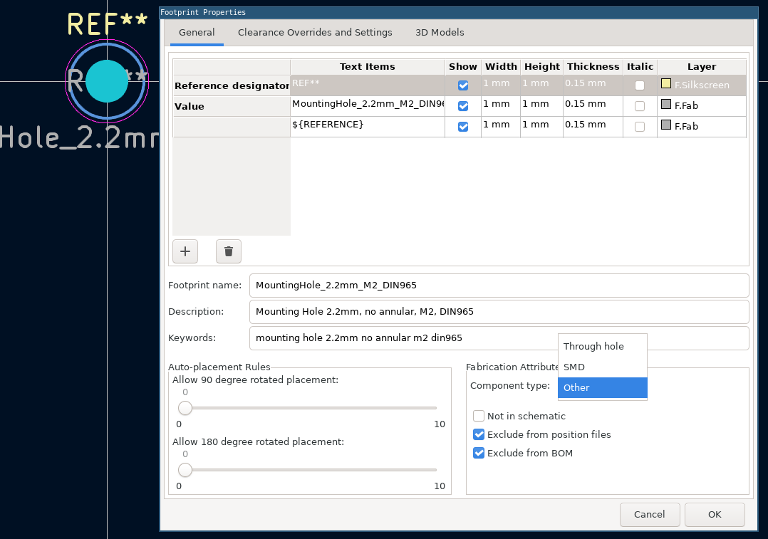
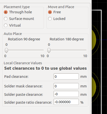
F4.6 Local clearance and settings should be set to zero
Pad clearance values are determined using a priority system, which checks the following locations for clearance values, in descending order of priority. If a particular setting reads as zero (0) then it is ignored, and the next location is checked.
-
Local pad settings - If an individual pad specifies clearance values, these are used
-
Footprint settings - If clearance values are specified in the Footprint Properties window, these are used
-
Global settings - If no values are specified as above, then the global values (as specified in PCB settings dialog) are used.
Unless there is a specific reason for setting explicit values for local clearance values for pads or pins, they should be left at zero (0).
Exceptions:
If the component datasheet calls for specific clearance values for a particular pad (or the entire footprint) then these values should be used as appropriate.
F5 - Layer Requirements
F5.1 Silkscreen layer requirements
The silkscreen is printed to the external surface of a PCB to aid in component identification and orientation. Typically this layer contains the component RefDes to locate components on the board after assembly.
KiCad refers to the silkscreen layers as:
-
F.SilkS- Front silkscreen layer -
B.SilkS- Back silkscreen layer
The following elements must be provided on the silkscreen.
-
Reference Designator must be drawn on
F.SilkSlayer-
Text size =
1.00mm -
Text thickness =
0.15mm
-
-
Silkscreen line width is between {
0.10mmand0.15mm}:-
Silkscreen line width should nominally be
0.12mm -
0.1mmis allowed for high density designs -
0.15mmis allowed for low density designs
-
-
Silkscreen must not be placed over pads or areas of exposed copper
-
Clearance between silkscreen and exposed copper elements is recommended to be 0.2mm.
-
Clearance must be at least the silkscreen line width or pad mask expansion, whichever is greater.
-
-
For SMD footprints, silkscreen must be fully visible after boards assembly (no silkscreen allowed under component)
-
For THT components, additional silkscreen may be placed under component to aid in assembly process
-
Polarity marking / Pin-1 designator must be drawn on the
F.SilkSlayer -
When components are expected to protrude past the board edge (e.g. connectors), silkscreen should not be placed such that a reasonably-placed component has silkscreen outside the board
-
Clearance between silkscreen and board edges should be at least 0.5mm
-
Polarity marking / Pin-1 designator
-
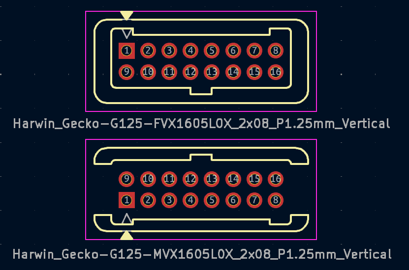
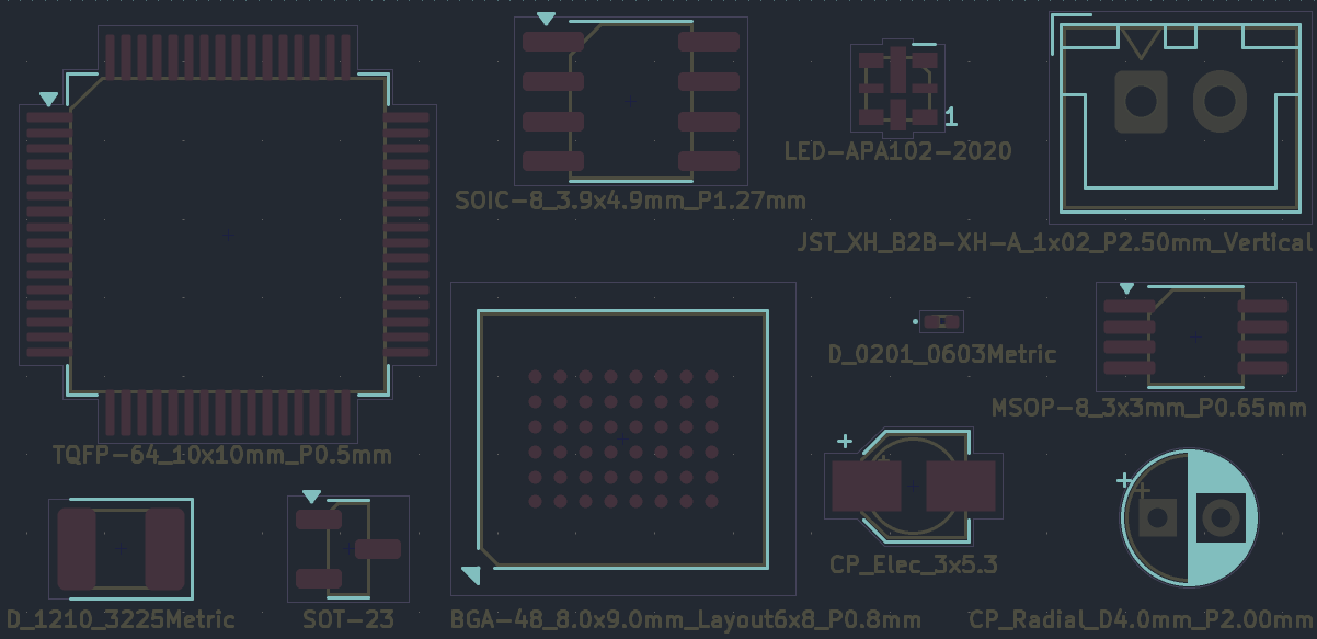
The prefered style for SMD packages is a filled chevron
▶-
It should positioned inside the courtyard to prevent silkscreen overlap
-
It can be rotated by 45° for a better fit
-
-
Examples other established and acceptable styles
-
for SMD devices
-
⊔shape for SMD diodes -
For small packages (0201 diodes, …) a 0.25mm dot should be used.
-
-
for THT and SMD packages
-
corner bracketorextra linefor connectors -
+sign for SMD capacitors
-
-
Follow established styles that already exist in the target library
-
-
If the device has a marking that is not on Pin-1 (popular on digital LEDs), the marking needs special attention
-
The digit
1is put on the silkscreen marker next to the pin numbered 1 -
The silkscreen polarity marking is placed according to the physical marking on the device
-
-
The marking must be visible after board assembly for inspection and debug purposes
-
It also should be visible after connector mating
-
Examples
Examples of silk for non-polarized components
Examples of silkscreen for polarized components
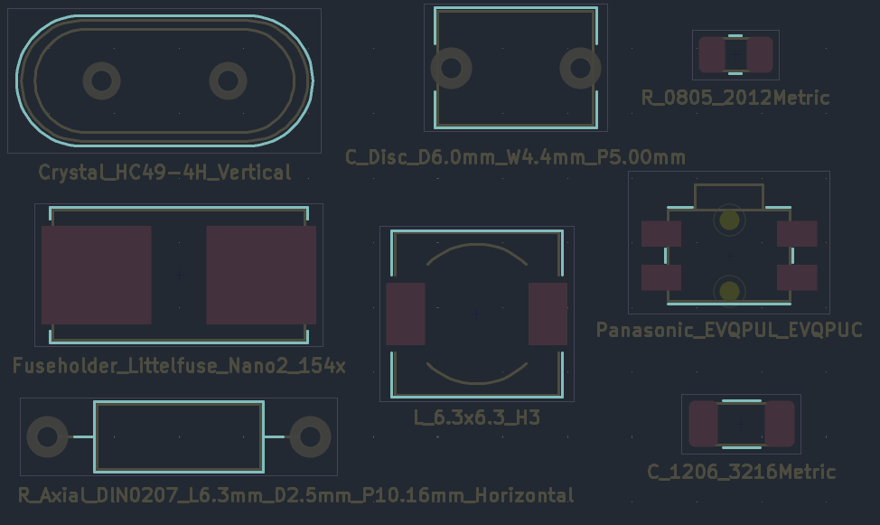
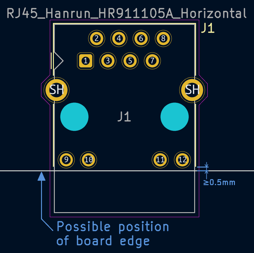
Example of a connector with silkscreen that is "pulled back" from possible board edges:
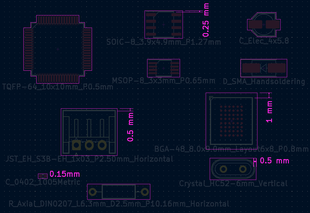
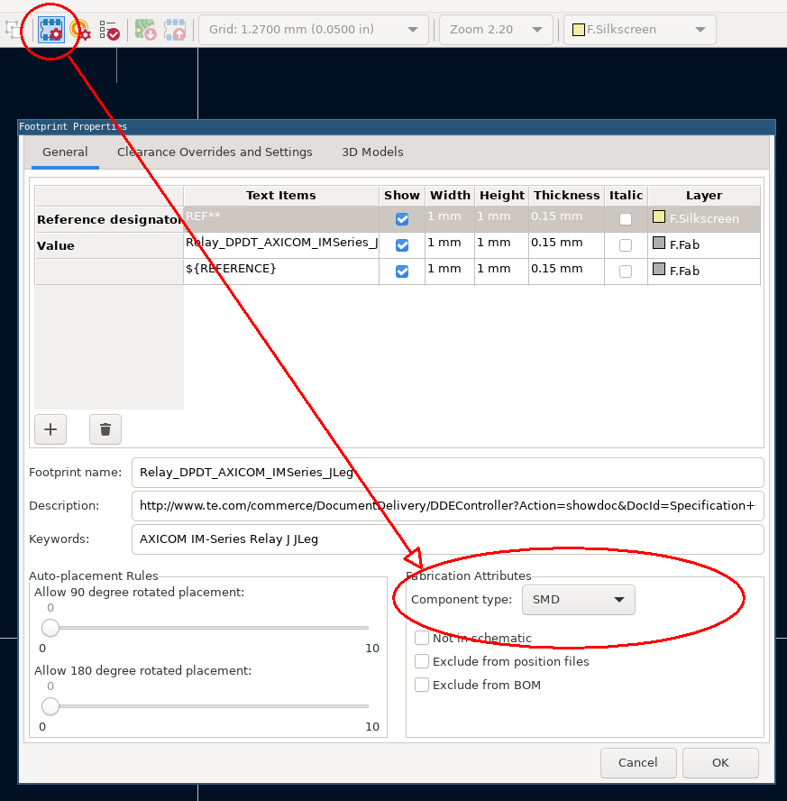
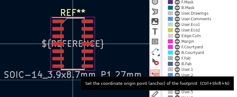
F5.2 Fabrication layer requirements
The fabrication layers are used to display the simplified mechanical outline of components on the PCB.
KiCad refers to the fabrication layers as:
-
F.Fab- Front fabrication layer -
B.Fab- Back fabrication layer
The following elements must be provided on the fabrication layer(s)
-
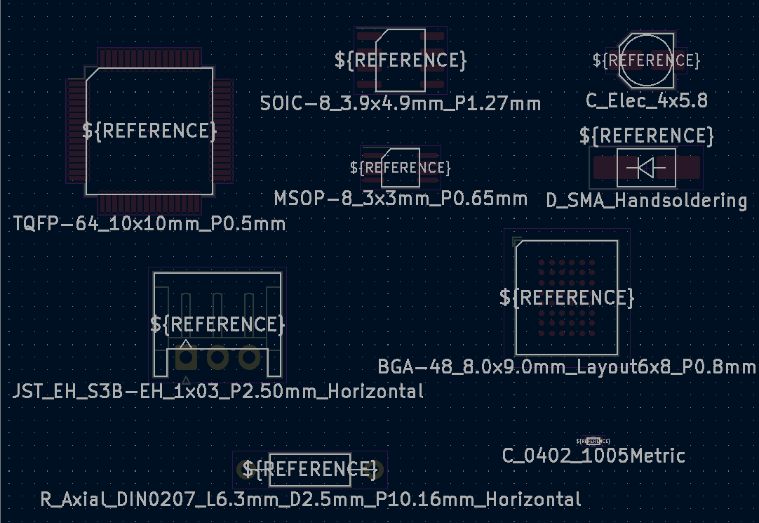
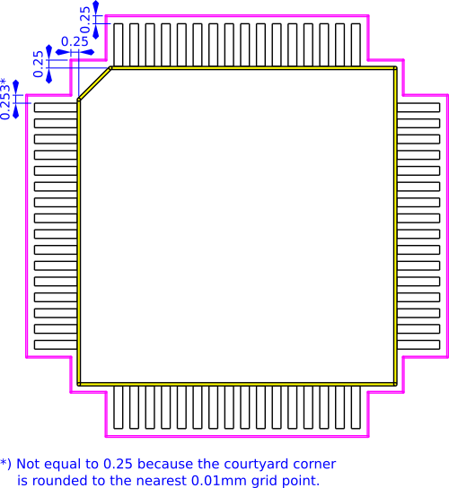
Simplified component outline must be provided on
F.Fablayer-
Outline uses line width between {
0.10mmand0.15mm} (recommended0.10mm) -
Outline should be simplified and not display complex features
-
For outlines based on the component body shape, the nominal size is used
-
-
Footprint polarisation / location of pin-1 is drawn
-
For IC packages, bevel is drawn at corner next to pin-1
-
Bevel should be
1mmor25% of package size(whichever is smaller) -
For connectors, a small arrow indicator drawn next to pin-1 should be used
-
-
Component value (footprint name) must be displayed on the
F.Fablayer-
Recommended text size =
1.0mm -
Allowable text size = {
0.5mmto1.0mm} -
Text thickness should be approximately
15%of text size ( with allowances for variation for aesthetic reasons) -
Placed below (positive y direction) the part outline.
-
-
A second copy of the reference designator (RefDes) must be provided on the
F.Fablayer. To add a second RefDes item, add a text object with the value${REFERENCE}-
RefDes must be centered on component body (inside component outline)
-
Orientation of RefDes should match major component axis
-
Size of text should be scaled to match component size
-
It is recommended to scale it such that 4 characters fit without overlapping other features of the same layer.
-
If it is not possible to fit at least 3 characters with the text size restrictions, then the reference should be moved outside (but scaled to smallest allowable text size)
-
-
Recommended text size =
1.00mm -
Allowable text size = {
0.5mmto1.0mm} -
Text thickness should be approximately
15%of text size (with allowances for variation for aesthetic reasons)
-
F5.3 Courtyard layer requirements
The component courtyard is defined as the smallest rectangular area that provides a minimum electrical and mechanical clearance around the combined component body and land pattern boundaries. It is allowed to create a contoured courtyard area using a polygon instead of a simple rectangle. (IPC-7351C)
The courtyard should include any extra required clearance for mating connectors (for example).
KiCad refers to the courtyard layers as:
-
F.CrtYd- Front courtyard layer -
B.CrtYd- Back courtyard layer
A fully enclosed Component courtyard must be drawn on the F.CrtYd layer, with the following parameters:
-
Courtyard uses
0.05mmline width -
All courtyard line elements are placed on a
0.01mmgrid -
If the component requires a courtyard on the back of the PCB, a corresponding courtyard must be provided on the
B.CrtYdlayer. -
Where the courtyard depends on the dimensions of the physical part body, clearance is calculated from the nominal part dimensions.
Courtyard clearance should adhere to the following requirements:
-
Unless otherwise specified, clearance is
0.25mm, this shrinks to0.15mmfor parts smaller than0603. -
(retracted)
-
Connectors should have a clearance of
0.5mm, in addition to the clearance required for mating of connector -
Canned capacitors should have a clearance of
0.5mm -
Crystals should have a clearance of
0.5mm -
BGA devices, including WLCSP and similar, should have a clearance of
1.0mm.
Example for courtyard clearance when applied to the contoured courtyard outline of a QFP-64 package. (Shown are courtyard, fab-outline and copper pads.)
F5.4 Elements on the graphic layer should not overlap
Footprints should not have overlapping or duplicate graphic elements. This includes lines, arcs and circles. Touching endpoints or intersections are not considered as overlapping.
F6 - Surface Mount Components
F6.1 Footprint component type must be set to surface mount
The Component type must be set to SMD for surface-mount footprints. This is to ensure that these footprints are included in the Footprint position (.pos) file output.
-
The checkboxes
Not in schematic,Exclude from position filesandExclude from BOMmust be unchecked -
To set the footprint placement type, open the Footprint properties window and select Surface Mount as indicated.
F6.2 Footprint anchor should be placed in the middle of the component body
The footprint anchor (also called component origin) is used by automated Pick and Place (PNP) machines for locating and placing SMD components on a PCB.
For most standard components, the anchor should generally be located on the centroid of the component body.
In the KiCad footprint editor, the footprint anchor is always located at the origin (0, 0). To move the footprint relative to the anchor (origin), press the Place footprint reference anchor button (refer to image below).
Exceptions:
Some footprints (especially those which are non-symmetrical) require special consideration and the anchor may not necessarily be placed on the component centroid.
Generally speaking, the correct location of the footprint anchor can be found in the component datasheet. The image below shows an example for a Molex Pico-Lock connector.
F6.3 Pad requirements for SMD footprints
Surface mount pads have specific requirements for PCB design.
-
By default, pads for SMD footprints should use only the following layers
-
F.Cu- Front copper -
F.Mask- Front soldermask -
F.Paste- Front solderpaste (stencil openings)
-
-
If SMD pads are placed on the back of the PCB, then the following layers should be used:
-
B.Cu- Back copper -
B.Mask- Back soldermask -
B.Paste- Back solderpaste (stencil openings)
-
-
Pads with specific stencil aperture design requirements require special attention (see details below)
-
Rectangular pads should use the "rounded rectangle" pad shape.
-
Exception: when the pad has a "trimmed heel" (perhaps due to a large thermal pad or a component body that would interfer with solder paste), use a rectangular pad
-
NOTE IPC-7351C recommended a radius of 25% of the shorter pad edge, or 0.25mm, whichever is smaller. IPC-7352 does not specify a radius, but this IPC-7351C recommendation is a good starting point.
Requirements for solderpaste
Many components (IC packages in particular) have specific design requirements for solderpaste (stencil) design. These requirements are often found in the footprint datasheet or an associated technical document.
Most often, custom stencil openings are required for the exposed pads on large IC packages to reduce the amount of solderpaste that is applied during stencil application.
The image below shows an example stencil design found in a footprint datasheet. The superimposed blue square represents the shape of the exposed copper pad. The green squares are the required openings in the stencil.
Custom stencil openings are accommodated as follows:
-
Construct copper shape with pad(s) with only copper layers (
F.Cuand/orB.Cu) as appropriate. These copper pads should not have theF.PasteorB.Pastelayers checked. -
Add stencil opening(s) with pad(s) which only use solderpaste layers (
F.Pasteand/orB.Paste) as required. These pads do not have a pad number. Set the pad type to SMD Aperture to disable the copper layer of the pads. -
The solderpaste should cover between 50% and 80% of the soldermask free pad area. (recommendation: 65%)
Result: (note: this footprint does not correspond to the example shown above)
Size of exposed pads
The following rules apply for finding the correct pad size for parts including an exposed pad.
-
By default the nominal size of the package pad is used.
-
Variation within the tolerance ranges of said package pad are allowed if the manufacturers suggested footprint suggest it that way.
-
It is not allowed to use a footprint pad smaller than the minimum size of the package pad.
-
Soldermask defined pads are to be used if the suggested footprint uses a pad larger than the maximum size of the package pad. (Meaning: copper can cover a larger area, but the exposed copper is still within the package pads tolerance range.)
-
Clearance requirement between exposed pads and normal pads
-
There should be clearance of at least 0.2mm between the exposed pad and the normal pads.
-
This clearance applies only to the area free of soldermask. (The clearance for soldermask defined pads is the spacing between the normal pads and the soldermask cutout of the exposed pad.)
-
The heel fillet of the normal pads is to be decreased if necessary to achieve this clearance.
Pad fabrication property
-
Heatsink pads (e.g. where an exposed pad is connected) must have the "heatsink" pad fabrication property set on the copper pads (front and, if present, back), as well as all thermal vias.
-
BGA pads where balls attach must have the "BGA" pad fabrication property set.
Zone connection overrides
-
Heatsink pads and thermal vias must have their zone connection override set to "solid".
F7 - Through Hole Components
F7.1 Footprint placement type must be set to Through Hole
The footprint placement type must be set to Through Hole for THT footprints. This ensures that these footprints are not included in the Pick and Place (PNP) location files.
This can be selected in the Footprint Properties window
F7.2 Footprint anchor should placed at the location of Pin-1
F7.3 Pin 1 should be rectangular or a rounded rectangle. Other pads circular or oval
Through hole components should set the shape of Pin 1 to Rectangular or Rounded Rectangle, and all other pads to either Circular or Oval.
This aids in orienting the component during placement and also for locating Pin 1 for circuit troubleshooting.
For rounded rectangle pads the corner size should be 25% with a maximum radius of 0.25mm.
Pad shape can be adjusted in the Pad Properties dialog:
Exception:
Non polarized parts (such as THT resistors) should not set the shape of Pin 1 to Rectangular. For these (non polarized) footprints, all pad shapes should be consistent.
F7.4 Pad requirements for THT footprints
Through hole pads must have soldermask pulled back to allow soldering. However they must not have solderpaste openings as they do not receive solder paste during stencil screening.
-
Pads for THT footprints must have the following layers set:
-
All copper layers
-
F.Mask(front mask) -
B.Mask(back mask)
-
-
Pads must not have the silkscreen layers active
F7.5 Minimum annular ring width
For drilled through-holes, the minimum annular ring width must be at least 0.15mm (IPC-2221).
The annular ring is the copper pad which remains after the hole has been drilled.
F7.6 THT hole diameter
-
Hole sizes refer to the finished hole size after plating (as opposed to the drill size before plating)
-
For soldered through-hole pads, minimum hole diameter is the maximum lead diameter plus
0.2mm -
This is derived from IPC-2222 class 2 recommendations
-
Maximum lead diameter is obtained from the device datasheet, and includes tolerances.
F7.7 Oval holes (plated milled slots)
The sizes for oval holes must be chosen such that there is 0.2mm clearance between the maximum lead size and the hole in all directions. Oval holes are only allowed if the lead length to width ratio is greater than 2. (Lead cross section is at least twice as long as wide)
Maximum lead dimensions are obtained from the device datasheet.
Some PCB manufacturers are not able to produce milled slots. It is allowed to add an alternative footprint using only circular holes. These need to follow the same drill size increase as all other holes. The equivalent lead diameter should be rounded up to the next 0.01mm increment.
The footprint name of such an alternative is marked with the suffix _CircularHoles.
F8 - Virtual Components
F8.1 Non SMD/THT components
Components which have a footprint on the PCB (and may additionally have a schematic symbol) but do not have an associated physical component which needs to be loaded onto the board during assembly must have their type set to Other.
The Exclude from position file checkbox must be marked, the Exclude from BOM checkbox should be checked.
Examples include:
-
Mounting holes
-
Solder bridges
-
Net ties
-
Test points
-
Fiducial markings
-
Symbols and Logos
Exclude from BOM
Some parts should be in the BOM, but not in the position file. Use this for components that need to be mounted manually.
For those, the Exclude from BOM checkbox must stay unchecked.
Examples include:
-
Lightpipes
-
Screws
-
Clip-on heatsinks
F9 - Footprint Properties
F9.1 Footprint meta-data is filled in as appropriate
-
Reference field must be set to
REF** -
Value and Footprint Name fields must match footprint filename (ignoring the
.kicad_modextension) -
Description field contains comma-separated device information. Where appropriate, a URL to the footprint datasheet should be included.
-
Keywords field contains space-separated keyword values
F9.2 Footprint properties are as default values unless otherwise required in datasheet
Footprint properties should be left as default, unless there is a reason to do so as specified by the footprint datasheet (for example).
-
Move and Place must be set to
Free -
Auto Place should be set to
0,0 -
Local Clearance Values should all be set to
0
Exceptions:
The Local Clearance Values parameters are generally set to 0, indicating that the global clearance values will be used to determine pad clearances.
If all the pads on the particular footprint require a specific clearance value (for e.g. as described by the datasheet) then these values can be used here to override pad-specific settings for the entire footprint.
F9.3 Footprint 3D model requirements
-
All non-virtual footprints must have 3D model references, even if the 3D model is missing (does not yet exist). This allows the 3D model to be added later without requiring the footprint to be edited again. (It is not required to supply a 3d model file.)
-
3D model files must be placed in a library (directory) which has the same name as the footprint library, with the extension
.3dshapes-
Capacitor_SMD.pretty→Capacitor_SMD.3dshapes -
Connector_USB.pretty→Connector_USB.3dshapes
-
-
3D model files should be named the same as the footprint (ignoring file extension)
-
SOIC-8.kicad_mod→SOIC-8.step -
R0805.kicad_mod→R0805.step
-
-
If a footprint is a simple variation that does not change the 3D representation, the common 3D model should be used (do not duplicate models unnecessarily)
-
R0805_HandSoldering.kicad_mod→R0805.step -
QFN-48_ThermalVias.kicad_mod→QFN-48.step
-
-
Model scaling must be 1:1:1 (model file should not require any scaling to correctly fit the footprint)
-
Rotation and offset must be 0 (The model must be aligned correctly to the footprint within the 3d modeling software.)
-
Path to 3D model must have the
${KICAD9_3DMODEL_DIR}/prefix -
Filetype must be
.step
3D Model Guidelines
The following guidelines apply to contribution of 3D model data.
M1 - Contributing Models
M1.2 The contributor must own the rights to share the 3D model
The goal of the KiCad 3d model library is to provide a free open library of 3d models. This requires certain restrictions regarding contributions with respect to their legal status.
-
Users must only submit models for which they own the rights allowing relicensing under the KiCad library licence.
-
In most cases this means they have created the model themselves, either manually designed in a parametric modeling software or via scripting tools.
-
Contributing model data designed by a third party complicates licensing issues and is to be avoided. This includes files downloaded from a manufacturers website.
M1.2 Withdrawn
This rule was withdrawn.
M1.3 Source files for 3D models must be supplied
The KiCad library maintains a repository for 3D source files at https://gitlab.com/kicad/libraries/kicad-packages3D-source.
The source files used to generate 3D model data must be submitted to this repository when a user contributes 3D model data.
-
Source files of 3d models are the native files generated by the 3d modeling software (Example: fcstd for Freecad).
-
Source files alternatively are any generator scripts.
-
However scripts found in https://gitlab.com/kicad/libraries/kicad-packages3D-generator do not need to be added to the source repo.
-
-
The source repository directory structure mirrors that of the kicad-packages-3d repository.
Exceptions
If the model is being submitted by an authorized representative of the manufacturer of the component, the requirement to also submit the source files may be waived by the KiCad Library team. This is contingent on the manufacturer providing the KiCad team with a primary point of contact to receive issue reports with the model as well as a commitment to providing updated STEP/WRL models that resolve issues with incorrect STEP/WRL models.
The KiCad Library team reserves the right to replace any models at their sole discretion and may prioritize models compliant with M1.3.
M2 - 3D File Requirements
M2.1 3D models must be supplied in both 'step' and 'wrl' formats
Any 3D model contribution to the KiCad library must be made in both step and wrl format.
WRL
-
WRL files contain material properties and are used for realistic rendering. However they cannot be exported to MCAD packages.
STEP
-
STEP files are used for integration with MCAD software packages. These files do not contain material properties and cannot be used for realistic rendering.
M2.2 Model alignment and scaling
The 3D models must be aligned and scaled appropriately to match the associated footprint.
Alignment
The 3D model must be aligned such that it does not require an additional alignment offset in the footprint options. When associating a 3D model with a footprint, the offset parameter must read (0, 0, 0)
Scaling
-
STEP files include absolute dimensional information, and must never have a secondary scaling factor applied. The model
scalingparameter in KiCad must read (1,1,1) -
WRL files do not specify absolute dimensions. The WRL fileformat has no way do specify what its units mean. KiCad considers one WRL unit to be 0.1 inches for historical reasons, so models must be scaled accordingly.
-
Assuming the model is designed in
mmthen the required scaling factor for WRL export is1/2.54(~0.393700787). -
The Freecad extension kicad-stepup exports WRL files already correctly scaled.
-
Rotation
The model must be rotated such that no additional rotation is required within KiCad to align the 3D model with the footprint.
M2.3 Freecad is the preferred design tool
The goal of the KiCad 3d model library is to provide a free open library of 3d models. The use of open source design tools is preferred for this very reason.
Freecad is chosen as the preferred tool to be used. Especially in combination with the kicad-stepup extension.
Good alternatives are open scripting options like OpenSCAD or CadQuery. For the latter consider contributing to https://gitlab.com/kicad/libraries/kicad-packages3D-generator
Files created in closed source tools are permitted. If a certain model is available designed in both an open and closed tool then the one from the open tool is preferred and will replace the other one.
KLC Exceptions
If a KLC rule was excepted for a Symbol a Property starting with "KLC_" and the KLC rule number afterwards, "KLC_S6.2", can let the automatic klc check know that this rule does not apply to this Object. A note about why this is exceptions is applied has to be added the property value.
This is not to be applied without discussion with a Librarian.
KLC Revision History
Revision information for the KLC can be found here.
