F6.3 Pad requirements for SMD footprints
Surface mount pads have specific requirements for PCB design.
-
By default, pads for SMD footprints should use only the following layers
-
F.Cu- Front copper -
F.Mask- Front soldermask -
F.Paste- Front solderpaste (stencil openings)
-
-
If SMD pads are placed on the back of the PCB, then the following layers should be used:
-
B.Cu- Back copper -
B.Mask- Back soldermask -
B.Paste- Back solderpaste (stencil openings)
-
-
Pads with specific stencil aperture design requirements require special attention (see details below)
-
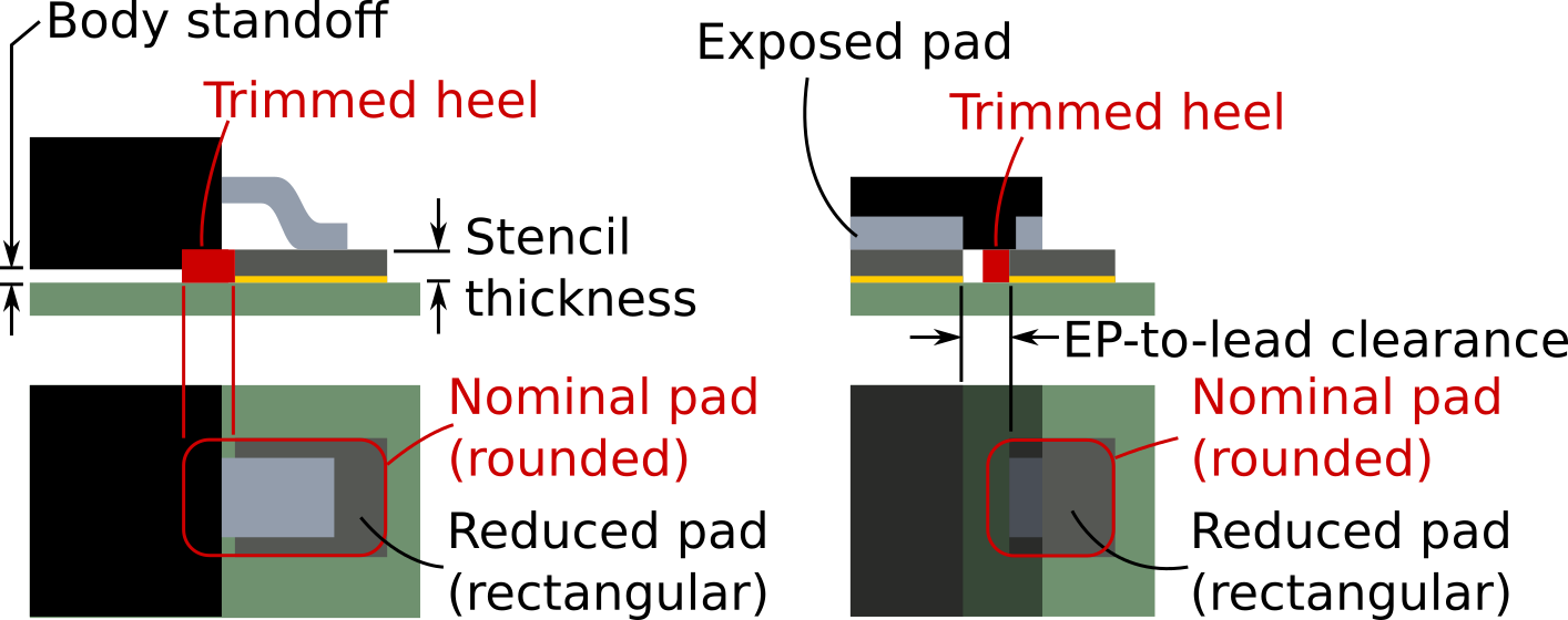
Rectangular pads should use the "rounded rectangle" pad shape.
-
Exception: when the pad has a "trimmed heel" (perhaps due to a large thermal pad or a component body that would interfer with solder paste), use a rectangular pad
-
NOTE IPC-7351C recommended a radius of 25% of the shorter pad edge, or 0.25mm, whichever is smaller. IPC-7352 does not specify a radius, but this IPC-7351C recommendation is a good starting point.
Requirements for solderpaste
Many components (IC packages in particular) have specific design requirements for solderpaste (stencil) design. These requirements are often found in the footprint datasheet or an associated technical document.
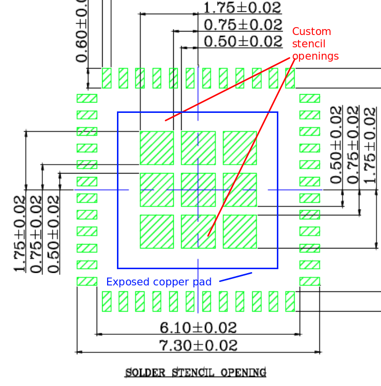
Most often, custom stencil openings are required for the exposed pads on large IC packages to reduce the amount of solderpaste that is applied during stencil application.
The image below shows an example stencil design found in a footprint datasheet. The superimposed blue square represents the shape of the exposed copper pad. The green squares are the required openings in the stencil.
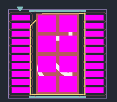
Custom stencil openings are accommodated as follows:
-
Construct copper shape with pad(s) with only copper layers (
F.Cuand/orB.Cu) as appropriate. These copper pads should not have theF.PasteorB.Pastelayers checked. -
Add stencil opening(s) with pad(s) which only use solderpaste layers (
F.Pasteand/orB.Paste) as required. These pads do not have a pad number. Set the pad type to SMD Aperture to disable the copper layer of the pads. -
The solderpaste should cover between 50% and 80% of the soldermask free pad area. (recommendation: 65%)
Result: (note: this footprint does not correspond to the example shown above)
Size of exposed pads
The following rules apply for finding the correct pad size for parts including an exposed pad.
-
By default the nominal size of the package pad is used.
-
Variation within the tolerance ranges of said package pad are allowed if the manufacturers suggested footprint suggest it that way.
-
It is not allowed to use a footprint pad smaller than the minimum size of the package pad.
-
Soldermask defined pads are to be used if the suggested footprint uses a pad larger than the maximum size of the package pad. (Meaning: copper can cover a larger area, but the exposed copper is still within the package pads tolerance range.)
-
Clearance requirement between exposed pads and normal pads
-
There should be clearance of at least 0.2mm between the exposed pad and the normal pads.
-
This clearance applies only to the area free of soldermask. (The clearance for soldermask defined pads is the spacing between the normal pads and the soldermask cutout of the exposed pad.)
-
The heel fillet of the normal pads is to be decreased if necessary to achieve this clearance.
Pad fabrication property
-
Heatsink pads (e.g. where an exposed pad is connected) must have the "heatsink" pad fabrication property set on the copper pads (front and, if present, back), as well as all thermal vias.
-
BGA pads where balls attach must have the "BGA" pad fabrication property set.
Zone connection overrides
-
Heatsink pads and thermal vias must have their zone connection override set to "solid".


